Nanochap BAF003 Analog Front-end on Smart Ring, Providing Smaller Size and Longer Battery Life

Smart ring is an innovative product that combines artificial intelligence and smart hardware technology, using the ring as a carrier to realize various functions of smart devices. With built-in sensors, chips, and connected devices, smart rings can realize various functions, such as detecting heart rate, blood oxygen, ECG, respiration rate, sleep condition, etc.

Fig.1
Smart ring has the advantages of smaller size and lighter quality than smart wearable products such as smart watches and smart wristbands, but these advantages also lead to higher requirements for the product's range and the size of the constituent parts, how to implant the detection chip and other components into a ring weighing a few grams and a few millimeters thick, and still guarantee a few days of range? Nanochap solved this problem with the Nine Senses BAF003 analog front end.
The Nine Senses BAF003 analog front-end uses a CSP package, highly integrated with six effects in one, with a volume of only 2.4mm, a standby current of less than 4 microamps, a PPG operating power consumption of 35 microamps, and an ECG of 39 microamps, which provides a long battery life.
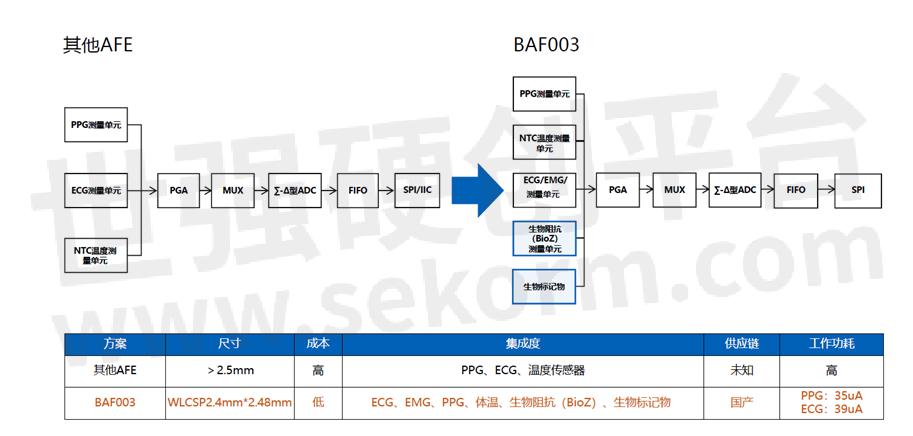
Fig.2
Nine Senses BAF003 analog front-end can be widely used in wearable devices for high-precision monitoring of heart rate, blood oxygen, blood pressure, body temperature, electrocardiographic parameters, electromyographic parameters and bio-impedance, etc., to manage related chronic diseases; and can also be used as an electrochemical sampling chip to measure various biomarkers in body fluids. BAF003 provides a high-precision and ultra-low-power solution for continuous monitoring of wearable medical products or consumer electronics.
Advantages and features of Nanochap BAF003 analog front-end
●Supports 3V power supply applications
●Leakage less than 15nA in disable mode.
●Ultra-low noise, high signal-to-noise ratio, two-stage programmable amplifier
●Acquisition circuit noise is less than 6μV
●Conversion accuracy of the effective number of bits to 16bit
Product parameters
●Supply voltage: 2.8V ~ 3.6V
●Package and size: WLCSP (2.4mm X 2.48mm)
●Op-amp bias voltage on-chip DAC (0.3V to 2V)
●Op-amp Noise: 2.2μV (0.1~10Hz)
●On-chip TIA feedback resistor: 200K ~ 10M 16 steps
●Programmable Gain Amplifier: 1st stage (1,2,3,4,8,16,32), 2nd stage (1,2,3,4)
●ADC precision: 16bit
●Chip sleep power consumption: <100nA
●Standby current: <4μA
●Continuous sampling power consumption: <40μA
●Temperature sensor: 0.1°C precision
●Application scenarios: ECG detection, blood oxygen detection, wearable devices, etc.
Chip structure diagram
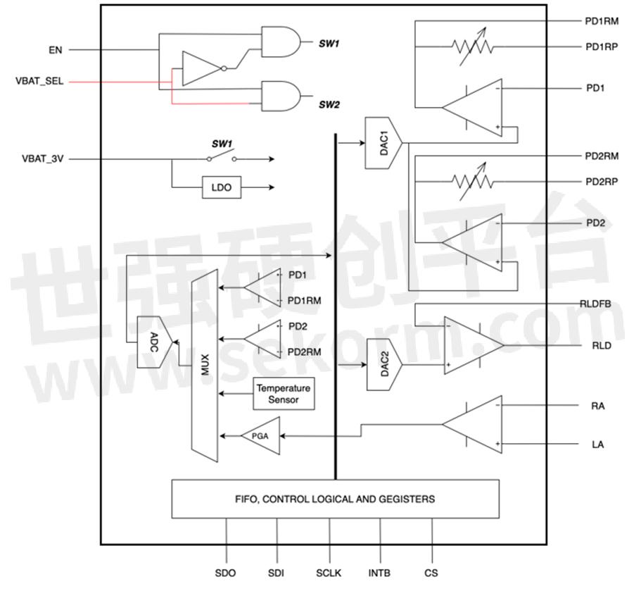
Fig.3
- +1 Like
- Add to Favorites
Recommend
- Nanochap Nine Senses Series BAF003 Analog Front-end in Wearable Sweat Sensor, Small Size, Long Life
- Nanochap‘s Physiological Signal Analog Front-End Chip BAF003 on Electrolyte Analyzer Characterized by Low Power Consumption
- Nanochap‘s BAF003 Physiological Signal Analog Front-end Chip for Intelligent Skin Detection Patches with Leakage Less than 15nA
- Warming up to the Use of Nanochap BAF003 Analog Front-end in Portable Impedance Detectors
- Nanochap Nine Senses Series BAF003 Analog Front-end Provides Strong Technical Support for the Myoelectric Test Trainer
- Nanochap BAF003 Analog Front-end on Disposable ECG Patches, Smaller Size and Longer Life
- Nanochap Launches Ultra-Low Power 6-in-1 Analog Front-end Biosignal Detection Chip - Nine Senses BAF003
- Nanochap Nine Senses Series BAF003 Analog Front End on Body Fat Scale Makes the Measurement More Accurate, Fast and Convenient
This document is provided by Sekorm Platform for VIP exclusive service. The copyright is owned by Sekorm. Without authorization, any medias, websites or individual are not allowed to reprint. When authorizing the reprint, the link of www.sekorm.com must be indicated.
Integrated Circuits


Discrete Components


Connectors & Structural Components


Assembly UnitModules & Accessories


Power Supplies & Power Modules


Electronic Materials


Instrumentation & Test Kit


Electrical Tools & Materials


Mechatronics


Processing & Customization


