Design Method of Analog Switch to Switch Audio Signal

The noise-canceling headphones, speakers, KVM, matrix, mixers, etc often require to processing of multiple audio signals. Designing a set of conditioning circuits for each audio signal will be very expensive and very complicated. The use of Analog switches for interleaving is obviously a very efficient approach.
The following design schemes are commonly used:
●Switching with an analog switch powered by a common single power supply
The signal range that ordinary analog switches can pass is -0.3V~VCC. For switching AC signals such as audio, DC bias voltage should be superimposed, that is, the signal must be raised above zero volts to pass reliably (Fig. 1). Each channel needs to add 3 resistance-capacitance components. If the signal has a DC bias voltage, it can be directly given to the analog switch.
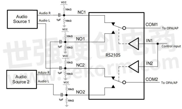
Fig.1 Ordinary switch RS2105 switches audio signals
●Analog switch with dual power supply
The analog switch with dual power supply, including an analog switch with a built-in negative voltage charge pump, the dynamic range of the signal that can be passed is broader, such as 74HC4051, support -VEE~+ VCC signal range, but requires additional components, which will increase the cost significantly.
●Use an analog switch with a negative swing capability
This is a type of analog switch with a negative swing designed specifically for AC signals, such as RS2117 and RS2118. The negative voltage signal that can be delivered under a single power supply can reach a maximum of -2V. Using this type of IC to switch audio signal circuits is the most efficient and cost-effective Higher (Fig. 2).
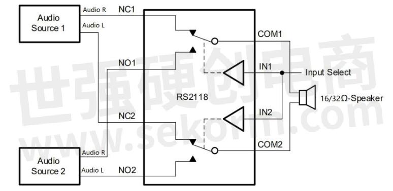
Fig.2 RS2118 switching audio signal
● With relay
Relay is the best choice for performance with small on-resistance and very good isolation, but they are bulky and expensive.
RS2117/RS2118 is a dual-channel single-pole double-throw (SPDT) analog switch of Runestone Technology. Its main features are as follows:
● -3dB bandwidth: 400MHz/RS2117, 80MHz/RS2118;
● Low on-resistance: 4.0Ω/RS2117, 0.8Ω/RS2118;
● Working voltage range: 2.5V~5.5V;
● Maximum pass signal range: -2V~VCC;
● Ultra-low power consumption:
● High shutdown isolation: -70dB@1MHz;
● High channel isolation: -72dB@1MHz;
● Provide QFN-1.4x1.8-10L small package.
Note: The smaller the on-resistance is, the larger the current that can pass. RS2118 is more suitable for switching with the load.

Fig.3 R2117/RS2118 pin diagram
Special attention needs to be paid to the design. The negative voltage signal range that RS2117/RS2118 can pass is subject to the VCC power supply voltage, that is, the negative voltage that can be passed is VCC-5.5V, the lowest is -2V, such as 3.3V power supply, the signal range It is -2V~3V.
- +1 Like
- Add to Favorites
Recommend
- Runic‘s OP Amp RS622,Analog Switch RS2105 and Low-Consumption LDO RS3236 Apply in Finger Clip Oximeter
- Runic Technology Launches Eleven Automotive-qualified ICs Meeting AEC-Q100 Grade 1 and MSL1
- Jiangsu Runic Technology Won 2021 China Analog Semiconductor Outstanding Business Award
- Runic Technology Participates in the 2021 ASPENCORE Double Summit
- The RS3005 Chip Developed by Runic Technology Helped The System MCU to Complete The Power Supply
- Runic OP Amp RS8551, LDO RS3002 and RS3226 Series Apply in Hand-Held Infrared Thermometer Detector
- Runic‘s OP Amp RS8538and RS622, Low-Consumption LDO RS3236 Apply in Electronic Blood-Pressure Meter
- Runic Low-power LDO RS3221 Assists in the Design of Smart Home Sensors and MCU Power Supply, With Small Package Size and Low Quiescent Current as Low as 1μA
This document is provided by Sekorm Platform for VIP exclusive service. The copyright is owned by Sekorm. Without authorization, any medias, websites or individual are not allowed to reprint. When authorizing the reprint, the link of www.sekorm.com must be indicated.
Integrated Circuits


Discrete Components


Connectors & Structural Components


Assembly UnitModules & Accessories


Power Supplies & Power Modules


Electronic Materials


Instrumentation & Test Kit


Electrical Tools & Materials


Mechatronics


Processing & Customization


