ROHM‘s High 8V Gate Withstand Voltage Marking Technology Breakthrough for 150V GaN HEMT

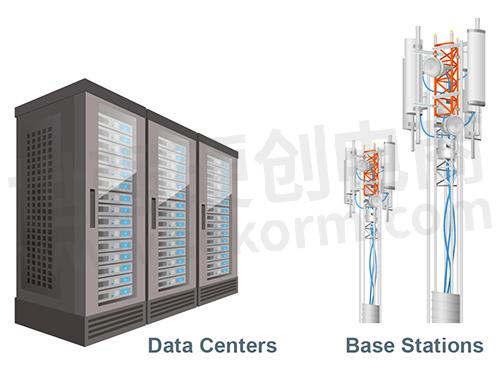
Solving the gate breakdown voltage problem of GaN devices contributes to lower power consumption and greater miniaturization of power supplies for base stations and data centers

ROHM developed the industry’s highest (8V) gate breakdown voltage (rated gate-source voltage) technology for 150V GaN HEMT devices – optimized for power supply circuits in industrial and communication equipment.
In recent years, due to the rising demand for server systems in response to the growing number of IoT devices, improving power conversion efficiency and reducing size have become important social issues that require further advancements in the power device sector.
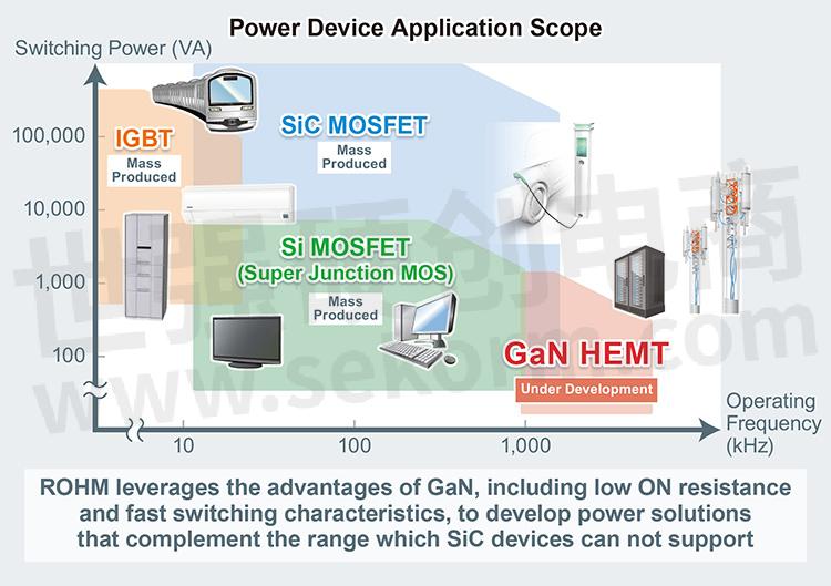
Along with mass-producing industry-leading SiC devices and a variety of feature-rich silicon devices, ROHM has developed GaN devices featuring superior high-frequency operation in the medium-voltage range. Cultivating technology that increases the rated gate-source voltage allows ROHM to propose a wider range of power solutions for a variety of applications.
As GaN devices provide improved switching characteristics and lower ON resistance than silicon devices, they are expected to contribute to lower power consumption and greater miniaturization of switching power supplies used in base stations and data centers. However, drawbacks include low rated gate-source voltage and overshoot voltage exceeding the max. rating during switching poses major challenges to device reliability.
In response, ROHM succeeded in raising the rated gate-source voltage from the typical 6V to 8V using an original structure. This makes it possible to both improve the design margin and increase the reliability of power supply circuits using GaN devices that require high efficiency. In addition to maximizing device performance with low parasitic inductance, we are also developing a dedicated package that facilitates mounting and delivers excellent heat dissipation, enabling easy replacement of existing silicon devices while simplifying handling during the mounting process.
Going forward, ROHM will accelerate the development of GaN devices based on this technology, with sample shipment planned for September 2021.

Key Features
ROHM’s newly developed GaN devices (under productization) offer the following advantages.
1. Original structure extends the rated gate-source voltage to 8V
Existing GaN devices with a withstand voltage of 200V or less typically have a rated gate-source voltage of 6V with respect to a gate drive voltage of 5V, resulting in an extremely narrow voltage margin of just 1V. Exceeding the rated voltage can cause reliability problems such as degradation and destruction, plus the gate drive voltage requires high accuracy control, which has been a major obstacle to the widespread application of GaN devices.
In response, ROHM succeeded in raising the rated gate-source voltage from the typical 6V to an industry-leading 8V by adopting an original structure. This triples the voltage margin during device operation, so even if a voltage overshoot exceeding 6V occurs during switching, the device will not degrade, contributing to higher reliability of the power supply circuit.
2. Optimized package provides excellent heat dissipation and facilitates mounting
ROHM’s GaN device utilizes a versatile package that delivers superior heat dissipation with a proven track record for reliability and accountability. This enables easy replacement of existing silicon devices and simplifies handling during the mounting process. Furthermore, using copper clip junction packaging technology reduces parasitic inductance by 55% over conventional packages, maximizing device performance when designing circuits for high-frequency operation.
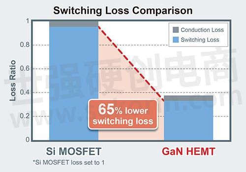
3. Reduces switching loss by 65% over silicon solutions Device performance is maximized by increasing the rated gate-source voltage and adopting a low-inductance package, resulting in 65% lower switching loss compared to the conventional silicon solution.
Application Examples
· 48V input buck converter circuits for data centers and base stations
· Boost converter circuits for the power amplifier block of base stations
· Class D audio amplifiers
· LiDAR drive circuits, wireless charging circuits for portable devices
Terminology
GaN HEMT
GaN (Gallium Nitride) is a compound semiconductor material used in next-generation power devices. It is beginning to see adoption due to its superior properties over silicon, such as excellent high-frequency characteristics.
HEMT stands for High Electron Mobility Transistor.
Rated Gate-Source Voltage (Gate Withstand Voltage)
Indicates the maximum voltage that can be applied between the gate and source. The voltage required for operation is called drive voltage. Applying a voltage above a certain threshold (drive voltage) will cause the GaN HEMT to become operational.
- +1 Like
- Add to Favorites
Recommend
This document is provided by Sekorm Platform for VIP exclusive service. The copyright is owned by Sekorm. Without authorization, any medias, websites or individual are not allowed to reprint. When authorizing the reprint, the link of www.sekorm.com must be indicated.
Integrated Circuits


Discrete Components


Connectors & Structural Components


Assembly UnitModules & Accessories


Power Supplies & Power Modules


Electronic Materials


Instrumentation & Test Kit


Electrical Tools & Materials


Mechatronics


Processing & Customization


