Solving Common Issues with Respect to PCIe Timing Design on the Modern Server System
Historically, servers aggregated timing onto a system board. Modern servers more commonly modularize the function and migrate the devices to different racks, like the tray of CPU, SSD, GPU, Accelerator, DRAM cards, etc., depicted in Figure 1.

Figure 1. Disaggregation system
Power cycling the system is a desirable capability, but in a disaggregated system, aligning both input signal and power sequences across the entire system becomes more complicated. Ideally, the system powers up consistently; but in practice, the time delta between power on and output clocks being ready to turn on varies. Let’s walk through some example cases relating to system clock design:
Case 1: No VDD
Figure 2 depicts a scenario where the motherboard sends its clock to other racks and add-in cards before power is ready. The clock buffers on the receiver side may start receiving the clock signal before their VDD turns on, thus outputting bad clock signals.

Figure 2. Wrong clock output when no VDD
Figure 3, depicts a scenario where the clock chip powers down during operation due to an emergency interruptions, like a system over-heat, hard reset, etc. A smart clock buffer can await a valid VDD prior to properly enabling the output.
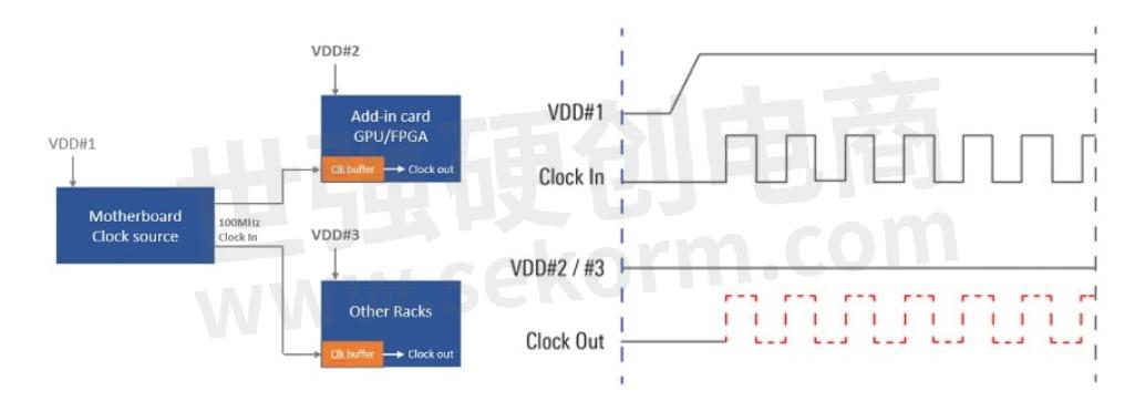
Figure 3. Wrong clock output when the system shutdown
Case 2: Noise Drives Oscillation on the Clock Buffer Output
If an add-in card or rack on the clocking receiver side powers up first, those on the receiver side won’t necessarily wait for a good clock source from the main motherboard. If your clock inputs are not carefully designed, you may trigger ESD events, or clock buffer outputs may start oscillating in response to that stimulus. A smart clock buffer has a mechanism inside to monitor the valid input clock source.

Figure 4. Noise input causes clock output oscillation
Case 3: Leakage Issue
Another common issue is that the output of a clock chip stalls at high/low or low/high state when the input reference clock disappears. HCSL topology has a natural shutoff characteristic that uses a low/low state when they are disabled. For LPHCSL topology, this may cause a problem without synchronizing an input reference clock to OE, power good or power down pins. In these cases, the system is supposed to be powered down, but the clock output may still be driving at 850mV as shown in Figure 5. Such leakage will add unwanted heat to the CPU. Smart clock buffers can force the outputs to a low/low state when there is no signal on the input.

Figure 5. Output is still driving at 850mV when no clock in
Helping customers address real-world scenarios such as these helped us to define such a smart buffer. Renesas’ new PCIe Gen6 RC190024/RC190020/RC190016/RC190013/RC190008/RC190004 clock buffer family and RC19216/RC19208/RC19204/RC19202 multiplexer family have built-in features to overcome all of these scenarios, including passive features like Power Down Tolerance (PDT), Flexible Startup Sequence (FSS) and (Automatic Clock Park (ACP). All of this is transparent to system designers but makes avoiding all of these possible gotchas easy during the design process.
- +1 Like
- Add to Favorites
Recommend
- Renesas DSP Solution on Renesas Lab on the Cloud, Input Analog Signals Directly From A Signal Generator To The Rx231 Microcontroller Evaluation Board
- Renesas‘ Semiconductor Manufacturing Factory (Naka Factory) Fire: Production Capacity Has Recovered to 88%
- Renesas Announces 10 New Winning Combinations Integrating Celeno and Renesas Products
- Renesas & Altran to Deploy First Social Distancing Wristwatch Using Ultra-Wideband Chipset with Low Rate Pulse
- Renesas and FAW Establish Joint Laboratory to Accelerate Development of Next-Generation Smart Vehicles
- Renesas Semiconductor Manufacturing Factory (Naka Factory)‘ Production Level Has Returned to 100%
- Renesas and Sequans Expand Their 5G Collaboration including Broadband IoT Module for 5G NR FR1/FR2
- Renesas and Cyberon Partner to Deliver Integrated Voice User Interface Solutions for Renesas RA MCUs Supporting Over 40 Global Languages
This document is provided by Sekorm Platform for VIP exclusive service. The copyright is owned by Sekorm. Without authorization, any medias, websites or individual are not allowed to reprint. When authorizing the reprint, the link of www.sekorm.com must be indicated.
Integrated Circuits


Discrete Components


Connectors & Structural Components


Assembly UnitModules & Accessories


Power Supplies & Power Modules


Electronic Materials


Instrumentation & Test Kit


Electrical Tools & Materials


Mechatronics


Processing & Customization


