Renesas Continues Leadership in Data Center with New Chipsets for High Performance Memory Modules Based on Multiplexed Rank DIMM (MRDIMM) Technology
Renesas Electronics Corporation, a premier supplier of advanced semiconductor solutions, unveiled the industry’s first server chipset for next-generation DIMM applications based on Multiplexed Rank DIMM (MRDIMM) technology. Even with the evolution of high-speed DDR5 specifications, many cloud and enterprise applications for in-memory databases, virtual machines and high-performance compute have insatiable appetite for memory bandwidth needs that native DDR5 technology cannot deliver. This is further accentuated due to the break-neck speed at which CPU core count is increasing. To alleviate this acute bottleneck on memory bandwidth, Renesas has collaborated with memory and CPU ecosystem vendors for over three years, playing a key role in architecture and specifications development for the new MRDIMM sub-system. Further, Renesas designed and executed two critical components – the RG5R188 Multiplexed Registered Clock Driver (MRCD) and the RG5F188 Multiplexed Data Buffer (MDB) – for the new architecture. Both components are available to partners to build the industry’s first memory modules based on MRDIMM technology.
MRDIMM technology employs an innovative, and powerful, yet simple concept to achieve significantly higher memory bandwidth. The host side connection to the CPU operates at twice the speed of the standard DDR5 DIMM. DRAM interfaces, however, operate at standard DDR5 speeds but fetch twice the amount of data from the DRAM with point-to-point post-buffer connectivity to the DRAM interface allowing both DRAM ranks servicing data to DB. This allows for the most cost effective and mainstream DRAM to be used for this purpose. Renesas’ MRDIMM chipset incorporates key functionality that manipulates the data between the host and DRAM interface at +135% bandwidth (BW) improvement over standard RDIMM (at 5600MT/s). It also optimizes signal integrity to achieve higher BW/watt with significant power optimization on the MRDIMM chipset.
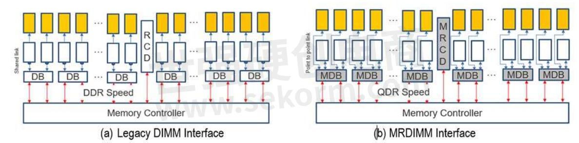
Figure 1. (a) Legacy DDR5 DIMM interface with shared link (b) MRDIMM interface with point-to-point link
MRCD is a Multiplexed Registered Clock Driver used on MRDIMMs to buffer the Command/Address (CA) bus, chip selects and clock between the host controller and the DRAMs. It also has a BCOM bus that controls the data buffers. MRCD contains two separate channels with some common logic such as clocking, but which otherwise operate independently of each other. For each channel, the host interface is a 7-bit + parity CA bus with two chip-select inputs. It is double data rate, carries two multiplexed pseudo-channels which can operate in the same direction simultaneously, and runs at twice the frequency of the DRAM interfaces. MRCD demultiplexes the pseudo-channels and transmits each to a separate DRAM output interface. Each DRAM interface is a 14-bit single data rate CA bus output with a chip-select. MRCD also transcodes commands from the CA bus onto a per-channel BCOM bus for data buffer control.
MDB is a Multiplexed Data Buffer to demultiplex and buffer data from the host CPU to DRAMs. It has two 4-bit data interfaces to the host, running at twice the speed of the DRAM interfaces. Each host interface multiplexes two pseudo-channels, both of which have a separate 4-bit DRAM interface. MDB supports x4 or x8 DRAMs. It also has an input-only control bus interface that is connected to an MRCD, as well as a dedicated pin for ZQ calibration and loopback outputs for test purposes.
- +1 Like
- Add to Favorites
Recommend
- Renesas DSP Solution on Renesas Lab on the Cloud, Input Analog Signals Directly From A Signal Generator To The Rx231 Microcontroller Evaluation Board
- Renesas‘ Semiconductor Manufacturing Factory (Naka Factory) Fire: Production Capacity Has Recovered to 88%
- Renesas Announces 10 New Winning Combinations Integrating Celeno and Renesas Products
- Renesas & Altran to Deploy First Social Distancing Wristwatch Using Ultra-Wideband Chipset with Low Rate Pulse
- Renesas and FAW Establish Joint Laboratory to Accelerate Development of Next-Generation Smart Vehicles
- Renesas Semiconductor Manufacturing Factory (Naka Factory)‘ Production Level Has Returned to 100%
- Renesas and Sequans Expand Their 5G Collaboration including Broadband IoT Module for 5G NR FR1/FR2
- Renesas Introduces Industry‘s First Industrial Temperature Grade DDR5 and DDR4 Registered Clock Drivers
This document is provided by Sekorm Platform for VIP exclusive service. The copyright is owned by Sekorm. Without authorization, any medias, websites or individual are not allowed to reprint. When authorizing the reprint, the link of www.sekorm.com must be indicated.
Integrated Circuits


Discrete Components


Connectors & Structural Components


Assembly UnitModules & Accessories


Power Supplies & Power Modules


Electronic Materials


Instrumentation & Test Kit


Electrical Tools & Materials


Mechatronics


Processing & Customization


