GaN Transistor for Several Power Applications

Silicon power MOSFETs have not kept pace with the evolutionary changes in the power electronics industry where factors such as efficiency, power density, and smaller form factors are the main demands of the community. The power electronics industry has seen the theoretical limit of silicon MOSFETs reached and now needs to move to a new element. Gallium Nitride or GaN is a highly mobile semiconductor electron semiconductor (HEMT) that is proving to be a real added value in meeting new applications.
GaN Transistors are significantly faster and smaller than silicon MOSFETs. The performance of GaN shows that efficiency and performance have improved significantly, leading to several new applications that were not possible with silicon technology. The board space is very expensive. eGaN® FETs, from EPC, are supplied in a low inductance, low resistance, small and low-cost LGA or BGA packages. In addition, they offer designers the best in class compared to MOSFETs in both hard switching and soft-switching applications.
GaN switching devices are available in two different types: enhancement mode (e-GaN) and cascoded depletion mode (d-GaN). An e-GaN works as a normal MOSFET, even if it has a reduced gate-to-source voltage. It offers a simpler package, a low resistance without a body diode with the bidirectional channel that behaves like this.
The d-GaN transistor is normally switched on and needs a negative voltage. You can overcome this problem by connecting the HEMT transistor in series with a low voltage silicon MOSFET, as shown in Figure 1.
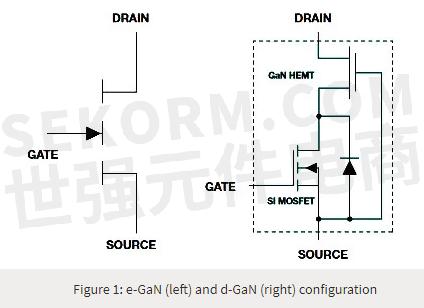
In contrast, the e-GaN transistor is normally off and is turned on with a positive voltage applied to the gate. e-GaN devices do not need a negative start-up bias unlike d-GaN: with a zero bias on the gate, the device is turned off and does not conduct any current.
The threshold of e-GaN FETs is lower than the one in silicon MOSFETs. This offers a very low gate-to-drain capacitance (CGD). Its structure with low capacitance permits switching hundreds of volts in nanoseconds with MHz frequencies. Gate-to-source capacitance (CGS) is another parameter that is large when compared to CGD, giving GaN FETs good dv/dt immunity. The dV/dt sensitivity of power-switching devices is caused by the various parasitic capacitances and gate-drive circuit impedances. The Gate-Charge Qg parameter, on the other hand, indicates the ability of the device to change quickly, reaching a higher dV/dT with minimal switching losses. e-GaN devices are 10x higher than MOSFET, while d-GaN devices are about 2x-5x higher.
To determine the dV/dt sensitivity of a power switch, you can use a figure of merit called the Miller charge ratio (QGD/QGS1). One Miller charge ratio less of 1 will guarantee the theoretical dV/dt immunity. The gate-drive circuit layout becomes a critical factor in improving dV/dt immunity.
The d-GaN transistor has the gate of a low voltage silicon MOSFET. Therefore, existing commercial MOSFET gate drivers can easily operate the d-GaN switch. An unfavourable effect with d-GaN devices is the higher ignition resistance due to the addition of the silicon MOSFET ignition resistance. The increase can be significant for low voltages (<200 V). For higher values (600 V), the additional resistance can only be about 5% of total resistance-on.
A d-GaN transistor has increased packaging complexity. Parasitic inductance and capacitance between the Mosfet device and GaN HEMT may cause delay during switching transients. The reverse conduction characteristics of a device are important in switching types. In a MOSFET, the voltage drop of a body diode is low, its reverse recovery is very slow, resulting in significantly high switching losses.
GaN devices do not have a reverse body diode but are able to conduct in the reverse direction due to its physical nature. In the case of reverse conduction, it will be necessary to have dead time. A d-GaN device in cascade have reverse recovery thanks to the low voltage silicon connected in series MOSFET.
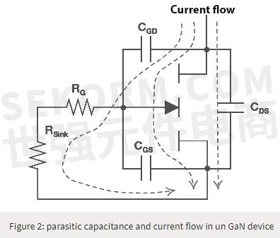
In hard-switching converters, the output charge is dissipated in the FET at each power-on transition. This loss is proportional to the QOSS, bus voltage, and switching frequency. GaN FETs have a significantly lower QOSS than silicon FETs, reducing the output charge loss per cycle and thus allowing higher frequencies (figure 2).
Solutions for Automotive and consumer
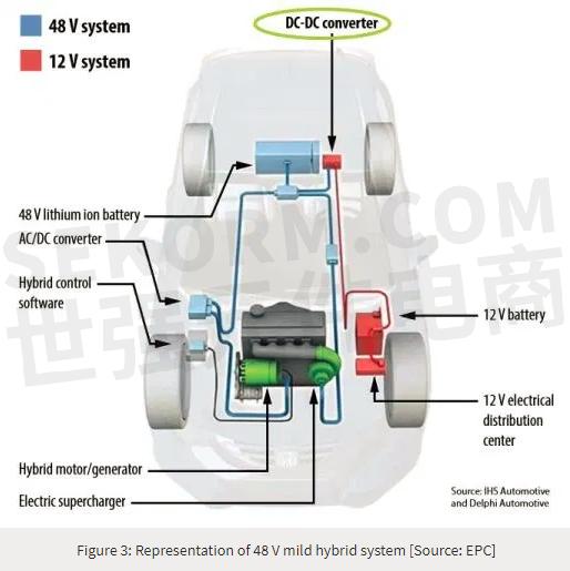
Emerging computing applications demand more power in much smaller form factors. In addition to the expanding needs of the server market, some of the most challenging applications are multi-user gaming systems, autonomous cars, and artificial intelligence Automotive systems are increasingly moving towards 48 V devices, driven by the increase in electronically controlled energy-hungry functions and the emergence of autonomous vehicles that create additional demands from systems such as lidar, radar, cameras and ultrasonic sensors on the energy distribution system. These processors are “energy-hungry” and represent an additional burden for traditional 12 V power distribution buses in the automotive sector. For 48 V bus systems, GaN technology increases efficiency, reduces system size, and reduces system cost. A 250 kHz GaN solution with double the frequency allows a 35% reduction in size, resulting in reduced inductor DCR losses, as well as cutting system cost by approximately 20% compared to the MOSFET solution. Gallium Nitride’s exceptionally high electron mobility and low temperature coefficient allows low QG and zero QRR. The final result is a device that can manage tasks with very high switching frequency, and low on-time are beneficial as well as those where on-state losses dominate.
“High power EPC eGaN® FETs offer lower resistance in the On state, lower capacitance, higher current, and excellent thermal performance characterize these power converters with over 98% efficiency. This family of eGaN FETs halves resistance (RDS(on)) to enable high current and high-power density applications.” Said Alex Lidow Ph.D. CEO and Co-founder at EPC.
The latest generation of eGaN FETs also halves the hard-switching Figure of Merit compared to the previous generation for improved switching performance in high-frequency power conversion applications. An increase in performance advantages of GaN to 30 V can be used to build high power DC/DC converters, PoL converters, and synchronous rectifiers for isolated power supplies, PCs and servers.
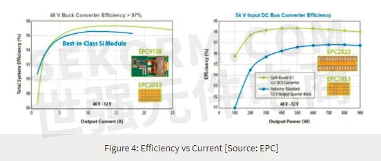
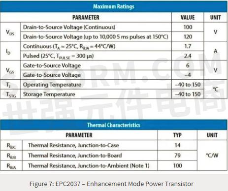
The smallest, most cost-effective and highest efficiency non-isolated 48 V – 12 V converter, suitable for high-performance computing and telecommunication applications, can be achieved by employing eGaN® FETs such as the EPC2045. EPC2045 has an operating temperature di -40 to +150 °C with Thermal resistance di 1.4 °C/W. The drain-source on-resistance is 5.6 mΩ typical (figures 3 and 4).
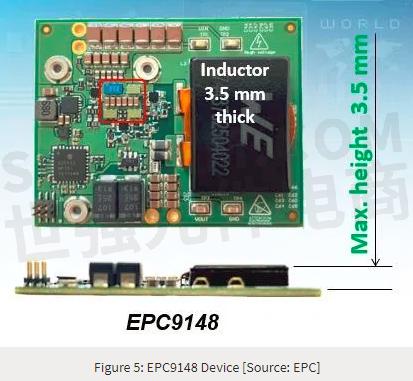
In the consumer market, portable solutions are becoming increasingly “energy-hungry”. It is very important to be able to manage efficiency and thermal management considering the small size of a laptop, sometimes with cooling solutions sometimes almost zero. The need for fast and efficient chargers has led the market towards new GaN solutions (figure 5).
Lidar
eGaN® FETs and integrated circuits are the logical choices to use when turning on a laser in a lidar system because FETs can be activated to create high current pulses with extremely short pulse widths. “The short pulse width leads to higher resolution, and the higher pulse current allows lidar systems to see further. These two features, together with their extremely small size, make GaN ideal for lidar,” said Alex Lidow.
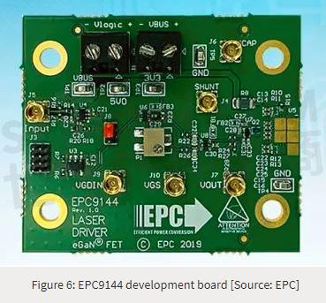
EPC provides various development boards. The EPC9144 is mainly designed to drive high current laser diodes with high current pulses with a total pulse width of 1.2 ns and currents up to 28 A. The board is designed around the 15 V EPC2216 eGaN® FET automotive-qualified AEC-Q101. The EPC9126 and EPC9126HC development boards are primarily intended to drive laser diodes with high current pulses with total pulse widths as low as 5 ns (10% of peak). They are designed with the 100V EPC2212 and EPC2001C enhancement-mode (eGaN®) field-effect transistor (FET), capable of 75 A and 150 A current pulses respectively. (figure 6).
Based on this technology, Helius, Cepton’s state-of-the-art lidar solution, delivers advanced object detection, tracking and classification capabilities to enable a wide range of applications for smart cities, transport infrastructure, security and more. It embodies an unprecedented fusion of three cutting-edge technologies: industry-leading 3D lidar sensing powered by Cepton’s patented Micro Motion Technology (MMT™); edge computing for minimum data burden and maximum ease of integration; and built-in advanced perception software for real-time analytics.
“Lidar has also become a very significant market. It is probably most recognized as the solution for autonomous cars. However, a faster-growing market is for short-range lidar which is being used for things like robots that only need see a few feet, drones for collision avoidance, and driver alertness systems . Short-range lidar systems do not require as much current as long-range lidar systems, but seeing the short distance means you need an even faster pulse. Because if you’re measuring something that is one meter away, that means the return signal will come back in just nanoseconds. We’ve demonstrated systems for short-range lidar that have pulse widths less than 1.2 ns.” Said Alex Lidow.
Wireless Power
“Wireless energy is ready to be incorporated into our daily lives.”, said Alex Lidow. Transmitters can be placed in furniture, walls, floors, to efficiently and economically power or charge our electronic and electrical devices over large areas and across multiple devices. The concept of wireless energy transfer has been known for some time, over 100 years to be precise, and dates back to the invention of the Tesla coil. A key factor in wireless energy transmission is efficiency: to be able to effectively define the system, a large portion of the energy transmitted by the generator must reach the receiving device.
Magnetic resonance technology is the key to ubiquitous implementation – enabling transmission over large areas, spatial freedom for positioning reception devices, and the ability to power multiple devices simultaneously.
EPC offers a full range of transmitter and receiver reference designs from single device charging to multiple devices powered simultaneously across a large surface area. GaN enables high efficiency for both the low frequency (Qi) and high frequency (AirFuel) standards supporting a lower cost; single transmit amplifier solution that can wirelessly charge devices regardless of the standard used in the receiving device. Wireless charging systems that rely on the Qi standard operate by inductive coupling at frequencies in the 100 to 300 kHz range.
Audio Applications
The lower power dissipation of Class D audio systems produces less heat, saves space and costs for printed circuit boards, and extends battery life in portable systems. GaN FETs provide higher fidelity Class D audio amplifiers. Recently however, as GaN-based high-electron-mobility transistor (HEMT) devices with much better physical properties have become a reality, a leap in Class D amplifier performance is on the doorstep.
The low resistance and low capacitance of eGaN® FETs offer low transient intermodulation distortion (T-IMD). Fast switching capability and zero reverse recovery charge enable higher output linearity and low cross over distortion for lower total harmonic distortion (THD).
“The First-Class D amplifiers were designed for cars, because they wanted to have more speakers and more power in cars. Class A amplifiers were just too big to produce more than about 25 Watts and still fit in the dashboard. Class D was first introduced in the 1980’s and enabled cars with 16 speakers and 250 watts of power. The sound quality, however, was never as good as a class A amplifier with Class D. That’s because MOSFETs can’t switch fast enough, and therefore, the relatively low switching frequency means relatively poor-quality reproduction. And with GaN devices, of course, you can go to much higher frequencies,” said Alex Lidow.
Space Applications
Gallium nitride, in its enhanced mode version (eGaN), is widely used in the development of for space applications. Commercial GaN power devices offer significantly higher performance than traditional Rad Hard devices based on silicon technology. This allows the implementation of innovative architectures with applications on satellites, data transmission, drones, robotics, and spacecraft.
eGaN FETs provide radiation tolerance, fast switching speed, improved efficiency, leading to smaller and lighter power supplies (smaller magnets and reduced heat sink size or even elimination of heat sinks in many cases). Power supply designers have the choice of increasing the frequency to allow smaller magnets, increase efficiency or design a satisfactory balance of both. eGaN FETs are also smaller than the equivalent MOSFETs. Faster transient response can also reduce capacitor size.
- +1 Like
- Add to Favorites
Recommend
This document is provided by Sekorm Platform for VIP exclusive service. The copyright is owned by Sekorm. Without authorization, any medias, websites or individual are not allowed to reprint. When authorizing the reprint, the link of www.sekorm.com must be indicated.
Integrated Circuits


Discrete Components


Connectors & Structural Components


Assembly UnitModules & Accessories


Power Supplies & Power Modules


Electronic Materials


Instrumentation & Test Kit


Electrical Tools & Materials


Mechatronics


Processing & Customization


