IV Characterization and Testing Considerations for Low-Power Integrated Circuits

Power Integrated Circuits (ICs) have become integral to virtually all electronic devices across diverse industries. These power ICs are pivotal in effectively managing, controlling, and monitoring power usage within these applications. As technology advances, the demand for highly sophisticated devices has increased, and correspondingly, the need for more power ICs within a single device has also risen.
According to ANA VILLAMOR, PH.D, Technology & Market Analyst, Power Electronics, from Yole Développement (Yole), ‘the total power IC market is expected to reach more than US$25.5 billion by 2026, with a CAGR of 3% between 2020 and 2026. (Yole)’s analysts have noticed that the power IC market has been extremely resilient over the last two years despite COVID-19, and this market saw year-over-year growth of almost 1.5% between 2019 and 2020 as consumer demand increased hugely.’

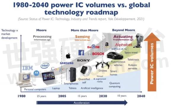
Figure 1. All products need power management to convert, control, monitor, or distribute power. (Source: Status of Power IC: Technology, Industry and Trends report, YoleDeveloppment, 2021)
Characterization and Testing Considerations for Power Integrated Circuits
To meet the ever-increasing demand for more sophisticated devices, these power ICs typically integrate additional components and functionalities to perform intricate tasks, consequently increasing the required test ports. This expansion in test ports ensures a comprehensive evaluation of the IC's performance, functionality, and reliability during the testing phase.
Moreover, these ICs are designed to operate at exceptionally low current and voltage levels, aligning with the strict requirements of low-power consumption. Wearables and smart devices or sensors, housing such ICs, often operate in multiple power states, including active, sleep, and idle modes, to conserve power and manage thermal effects.
Enhancing the robustness and efficiency of power ICs is a common endeavor. Accomplishing this task entails tackling the challenge of current-voltage (IV) characterization. It is imperative to achieve low power consumption to extend the lifespan of batteries, mitigate thermal effects, and maximize overall efficiency.
Additionally, the reliability of these circuits must be upheld to ensure they perform optimally in even the harshest operating conditions. As a result, manufacturers undertake IV characterizations under diverse operating conditions to validate circuit designs, identify potential faults, and optimize overall performance.
As such, the test engineers require dynamic and static DC IV characterization techniques to accurately assess the behavior of these ICs across different power modes. Consequently, these intricate requirements have resulted in more complex test sequences and the incorporation of additional test instruments.
Challenges in IV Characterization of Low-Power ICs
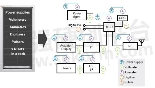
Due to the intricate nature of the test sequences, IV characterization for low-power ICs often demands extensive equipment and entails substantial costs. Engineers must employ multiple power supplies to provide the required voltages to various test ports with diverse voltage requirements.
Additionally, digital multimeters (DMMs) are necessary for precise voltage and current measurement, while pulsers are essential for simulating signals, and digitizers were used to capture signals in the time domain accurately. However, managing multiple instruments, particularly synchronizing these test instruments, can be a challenging and cumbersome experience. Adding dozens of channels to your test bench is not a scalable solution. Synchronizing multiple test instruments and ensuring efficient footprint allocations, sufficient test coverage, and reduced test time become increasingly important.

Figure 2. The number of test instruments required for a low-power IC IV characterization.
IV Characterization with Conventional SMU
A promising solution lies in utilizing a source measure unit (SMU) capable of serving as both a voltage and current source while simultaneously measuring voltage and current.
However, many conventional SMUs lack the inclusion of essential features such as pulsers and digitizers, which are crucial tools for accurately capturing signals, performing precise measurements, generating controlled signals, conducting timing analysis, and validating overall performance. These instruments play a pivotal role in ensuring the reliability, functionality, and efficiency of low-power ICs across diverse applications. Considering the complexities involved, reliance on multiple independent instruments would only exacerbate synchronization issues, failing to offer a comprehensive resolution.
Advanced Source Measure Units (SMUs) for Enhanced IV Characterization of Low-Power ICs
Advanced SMUs, which encompass all essential features required for accurate IV measurements, have emerged as a powerful solution to address the challenges faced by conventional SMUs in characterizing low-power ICs. These next-generation SMUs should be specifically designed to serve as both voltage and current sources while simultaneously incorporating pulsers, digitizers, and other necessary functionalities.
By integrating these essential tools into a single, versatile instrument, engineers can benefit from a streamlined testing process, minimizing synchronization challenges and reducing the need for multiple independent instruments. Such integrated SMUs will facilitate a more comprehensive and efficient testing approach, leading to significant time and cost savings in the characterization of low-power ICs.
In this regard, the Keysight PZ2100 stands as an exceptionally advanced source measure unit designed specifically to address the challenges mentioned above of low-power IC characterization. The Keysight PZ2100 offers a comprehensive solution with advanced features, enabling accurate IV characterization and efficient power management testing for low-power ICs.
- +1 Like
- Add to Favorites
Recommend
This document is provided by Sekorm Platform for VIP exclusive service. The copyright is owned by Sekorm. Without authorization, any medias, websites or individual are not allowed to reprint. When authorizing the reprint, the link of www.sekorm.com must be indicated.


