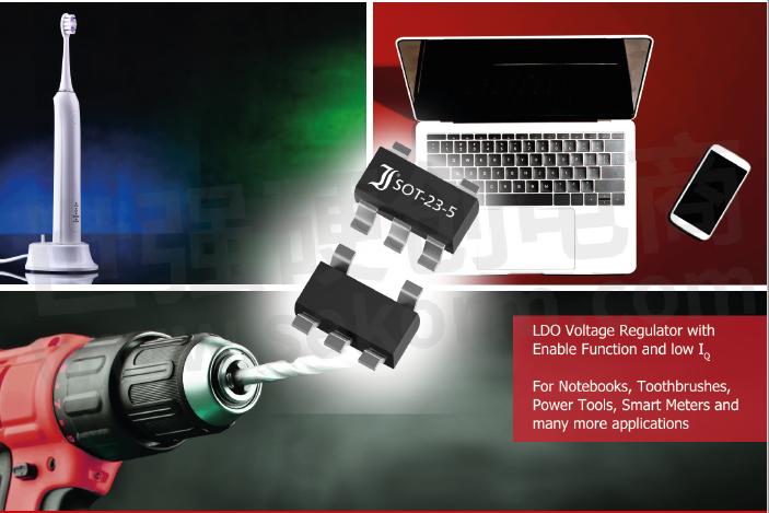
For Applications Where the LDO Voltage Regulator Operates Mostly Under No Load Conditions, the Quiescent Current Plays a Major Role

A low dropout LDO voltage regulator is a linear device that maintains a stable output over a wide range of input voltages and output currents. LDOs operate at low voltage differences between input and output. Furthermore, they can be used as noise reduction patches to solve voltage regulation problems caused by electromagnetic interference (EMI) and printed circuit board (PCB) routing. Luckily, the enable function allows switching the regulator on and off, thus improving the overall system efficiency by turning off unused functions.
Enabling
The Enable input (EN), available in positive and negative logic, turns the device on and off by an external signal. Active-high logic activates the device when the voltage at the EN-input exceeds the high-logic threshold. The active-low logic switches the device off when the EN-voltage falls below the logic low threshold. The EN-function is an important feature when sequencing power supplies in multi-rail systems. Keeping the internal bandgap reference running while the regulator is disabled allows for fast turn-on times.
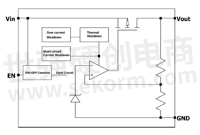
Figure 1: DIOTEC LDI8119-xxEN internal block diagram
Shutdown-Current and Quiescent current
When the LDO is turned off and connected to the battery system, the input current will be limited, usually up to 1 μA. This Shutdown current is commonly confused with the quiescent current which is the current drawn by the device when it is enabled and operating with no load. Both shutdown and quiescent current are important parameters when realizing long battery lifetimes in portable devices. Using the datasheet values for shutdown and quiescent current designers can calculate power dissipation as shown in the below equations.
For example, when the device is fully operational, the voltage is regulated from VIN 10.0 V to VOUT 5.0 V with an output current of 400 mA. The datasheet value for quiescent current is 60 μA. This will result in a power dissipation (PD) of:
Check again with new value for IQ
PD= (VIN-VOUT ) ∙ IOUT + (VIN ∙ IQ )
PD= (10 V - 5 V) ∙ 0.4 A + (10 V ∙ 0.00006 A)
PD= 2.0006 W
When the device is switched into no load operation, the output current falls as low as 200
μA. Then the PD becomes:
PD= (10 V-5 V) ∙ 0.0002 A + (10 V ∙ 0.00006 A)
PD= 1.6 mW
In this case, the quiescent current accounts for nearly 50% of the total power dissipation.In conclusion, the following is stated: For applications where the device operates mostly under no load conditions, the quiescent current plays a major role and should be considered when planning the design.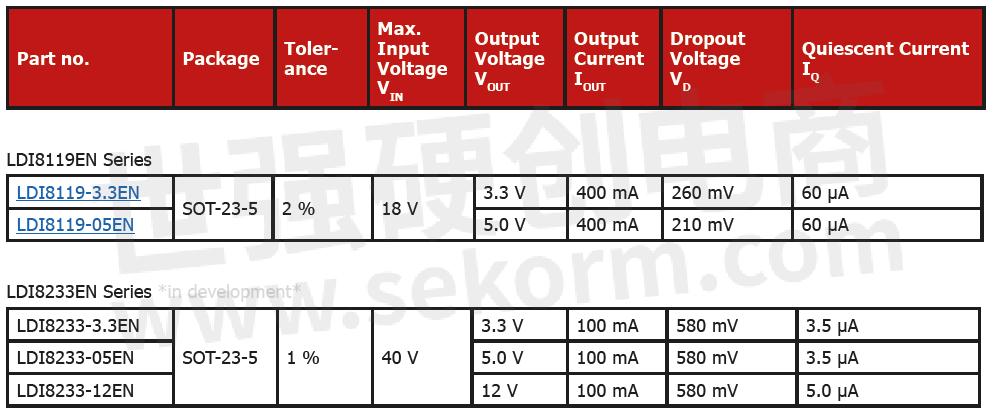
- +1 Like
- Add to Favorites
Recommend
- Diotec‘s New LDO Voltage Regulators LDI8119EN and LDI8233EN Help Prolong Battery Lifetime
- Headset with Diotec’s Voltage Regulator LDI8119-05EN Brings an Immersive Acoustic Gaming Experience
- Diotec‘s Product Portfolio Offer Discrete Solutions for EV Charging
- Diotec Linear Voltage Regulators - Stable Output Voltage at Low Costs
- Diotec Ultrafast Rectifier US1M——Why It Makes Sense to Use a 1000 V Component on a 24 V Smart Building Field Bus System?
- Diotec Offers Several Semiconductor Solutions Dedicated for Smart Meter Needs
- Diotec Bipolar Transistor BC847BP in the DFN1006-3 Package, Suitable for Many Kinds of Electronic Control Purposes in Toy Robots
- What Diotec Bipolar Transistor MMDT2227 Has to Do with Cheerful Coloured Eggs?
This document is provided by Sekorm Platform for VIP exclusive service. The copyright is owned by Sekorm. Without authorization, any medias, websites or individual are not allowed to reprint. When authorizing the reprint, the link of www.sekorm.com must be indicated.
Integrated Circuits


Discrete Components


Connectors & Structural Components


Assembly UnitModules & Accessories


Power Supplies & Power Modules


Electronic Materials


Instrumentation & Test Kit


Electrical Tools & Materials


Mechatronics


Processing & Customization


