How to Design a 2 kW 48 V/12 V Bi-Directional Power Module with packaged eGaN® FETs

By 2025, one of every 10 vehicles sold worldwide is projected to be a 48V mild hybrid. 48V systems boost fuel efficiency, deliver four times the power without increasing engine size, and reduce carbon-dioxide emissions without increasing system costs. These systems will require a 48V/12V bidirectional converter, with power ranging from 1.5kW to 6kW. The design priorities for these systems are size, cost, and high reliability.
This application note discusses the design of an EPC9165, 2kW, two-phase 48V/12V bi-directional converter using GaN FETs in QFN packages, achieving 96% efficiency. The heatsinking capability can be considered infinite since this will ultimately function inside a vehicle with the unit mounted to the chassis.
Design of the Bi-directional DC-DC converter
A simplified schematic of the EPC9165 bi-directional DC-DC converter is shown in Fig. 1. Since the synchronous buck/boost converter is the simplest bi-directional converter, it is selected as the base topology. Other supporting circuitry includes current sensors, temperature sensors, digital controllers,s and housekeeping power supply.
GaN FETs used in 48V applications usually have a 4 times better figure of merit (die area · RDS(on)) compared to similar MOSFETs. For the same gate voltage of 5V, GaN FETs have at least 5 times a lower gate charge than MOSFETs. Other important advantages of GaN FETs include lower COSS, faster voltage transition, zero reverse recoveries and they are physically smaller.
The eGaN FET EPC2302 is used in this design. It has a low inductance 3 x 5mm QFN package with an exposed top for excellent thermal management. With 1.8mΩ RDS(on), the rated peak DC current is 101A. Therefore, the two-phase approach is selected so that the FET current requirement is reduced, i.e., at 14V 2kW output, the DC current in each phase is 70A. This also reduces the current rating requirement for the inductors.
The MPQ1918-AEC1 gate drivers in this design are AEC-Q100 qualified and use a bootstrap technique with voltage clamping for driving high-side FET. They also have fast propagation times and excellent propagation delay matching of less than 1.5ns typical.
Vishay IHTH-1125KZ-5A series inductors offer high current ratings for the inductance. In this design, the 1.0µH inductor and 500 kHz switching frequency is selected, resulting in an 80A peak inductor current.
To ensure accurate phase current balancing, current sensing using precision shunt resistors is preferred over inductor DCR current sensing. However, shunt resistors rated for above 70A usually have a large footprint, and therefore high parasitic inductance. This inductance can produce high noise that saturates the current sense amplifier and voids the measurement. A simple solution is to add an RC filter network with a matched time constant. The MCP6C02 current sense amplifier is used in this design, with a maximum bandwidth of 500kHz and 50V/V gain. This results in 10mV/A total current sensing gain for a 0.2mΩ shunt.
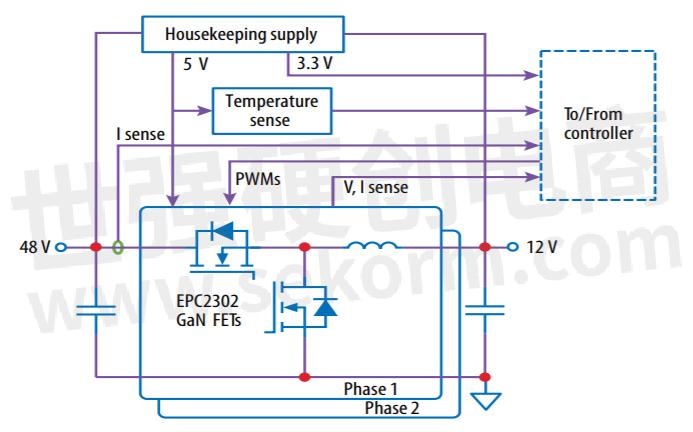
Figure 1. EPC9165 system block diagram
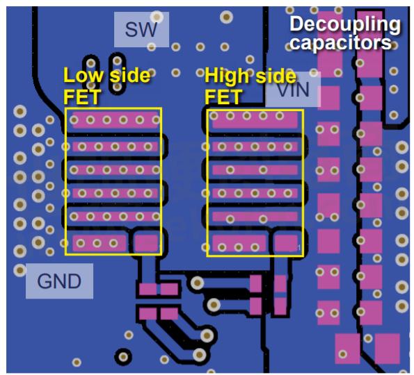
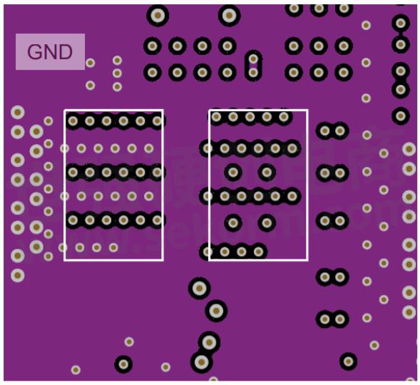
The symmetrical layout between the two-phase is also critical for phase current balancing and minimizing other effects from the mismatch, such as gate drive delay, switching transition speed, overshoot, etc. Figure 2 shows the layout example around the GaN FETs in this design, which utilizes the internal vertical layout technique by placing the decoupling capacitors close to the FETs with a solid ground plane underneath.
(a)
(b)
Figure 2. Example layout of the top two layers of the printed circuit board around GaN FETs:
(a) a top layer consisting of ground (GND), switching node (SW), and input (VIN) nets
(b) middle layer 1 of the solid ground plane.
Digital Control
A dsPIC33CK256MP503 digital controller from Microchip is used in this design. It is a 16-bit processor with a maximum CPU speed of 100 MIPS. The pulse-width modulation (PWM) module can be configured in high-resolution mode, resulting in 250ps resolution in duty cycle and dead times, allowing accurate adjustment of dead times to fully exploit the high performance of GaN FETs.
Digital average current mode control is implemented for both buck and boost modes. The current sensing circuitry consists of sense resistors and differential amplifiers. In this design, low loss 0.2mΩ sense resistors and low-noise amplifiers MCP6C02 are used. The control block diagram is shown in Fig. 3. The same current reference IREF is used for the two independent current loops. As a result, the current in both inductors will be regulated to the same value. The bandwidth of the two inner current loops is set to 6kHz, and the outer voltage loop bandwidth is set to 800Hz
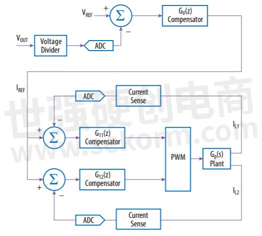
Figure 3. The digital average current mode control diagram
Thermal Management
At a full output power of 2kW, a heatsink is required for the GaN FETs. A standard commercially available 8th brick heatsink is used. Four metal spacers are installed on the PCB to provide the appropriate clearance for the heatsink mounting. A thermal interface material (TIM) is required between the FETs and the heatsink. Usually, the material needs to have a) mechanical compliance due to compression, b) electrical insulation and c) good thermal conductivity. In this design, a TIM with 17.8W/mK is used. Figure 4 shows the 3D heatsink installation view.

Figure 4. Heatsink installation view, showing the SMD spacers, thermal interface material
Performance Results
Figure 5 shows a photo of the EPC9165 converter without the heatsink mounted. The dimensions are 4.3 x 2.8 x 1.6 inches (108 x 70 x 40mm) excluding the edge connectors.
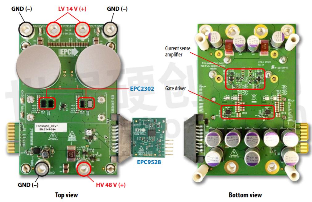
Figure 5. Photo of the EPC9165 converter with the EPC9528 dsPIC33CK controller module attached
With the heatsink installed and 1700 LFM airflow, the converter was operated at 48V input, 14.3V output and tested at 500kHz, and the efficiency results are shown in Fig. 6. At 500kHz, using a 1µH inductor, the converter achieved a peak efficiency of 97%. The converter was also tested at 14.3V input and 48V output for boost mode operation, as shown in Fig. 7.
At full load, EPC eGaN FETs can operate with 96% efficiency at the 500kHz switching frequency, enabling 1kW/phase compared to silicon-based solutions, which are limited to 600W/phase due to the limitation on the inductor current at 100kHz maximum switching frequency.
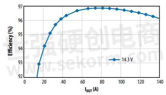
Figure 6. Measured converter efficiency at 500kHz, 48V input, and 14.3V output
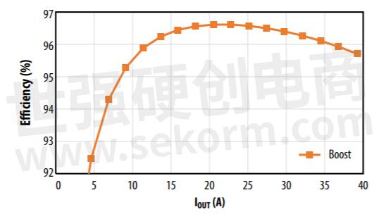
Figure 7. Measured converter efficiency at 500kHz, 14.3V input, and 48V output
Conclusion
This application note introduces a bi-directional high-power EPC9165 converter for mild-hybrid cars and battery power backup units using four EPC EPC2302 packaged eGaN FETs. When converting between 48V and 14.3V, the efficiency exceeds 96% with a 500kHz switching frequency. This design meets the priorities of size, cost, and high reliability that a 48V/12V bidirectional converter, with power ranging from 1.5kW to 6kW demands.
- +1 Like
- Add to Favorites
Recommend
This document is provided by Sekorm Platform for VIP exclusive service. The copyright is owned by Sekorm. Without authorization, any medias, websites or individual are not allowed to reprint. When authorizing the reprint, the link of www.sekorm.com must be indicated.
Integrated Circuits


Discrete Components


Connectors & Structural Components


Assembly UnitModules & Accessories


Power Supplies & Power Modules


Electronic Materials


Instrumentation & Test Kit


Electrical Tools & Materials


Mechatronics


Processing & Customization


