ATP‘s PCB Assembly Solderability Validation Tests

Overview of ATP’s PCB Assembly Solderability Validation Tests
Soldering is an important process to make sure that components on the printed circuit board assembly (PCBA) are effectively bonded to form reliable mechanical and electrical connections. Part of this process is called “wetting,” where the metal in the solder becomes molten fluid to bond and adhere with the metal components on the PCB. Evaluating solderability is the process of testing how well the solder secures those connections. This crucial process must be done before finalizing the PCB assembly, as poorly soldered parts can affect the PCB functionality, lead to defects, and incur more costs.
ATP PCB Assembly Solderability Validation
ATP performs solderability validation using temperature stress and external forces to validate the robustness of the soldering process.
The tests included in the solder process validation are described in this section.
Visual Inspection
●Automated Optical Inspection (AOI) – Typically performed after the soldering process, AOI is a non-contact method where a camera autonomously scans the PCB for surface defects, soldering flaws, and missing skewed, faulty, or misplaced components.
Pass/Fail Criteria: IPC-610 Specifications
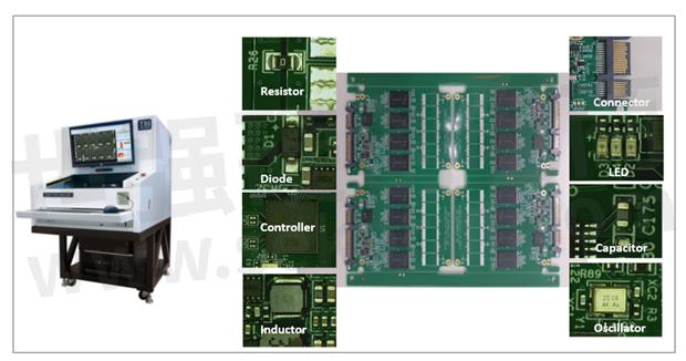
Figure 1. PCB items to be checked.
●Automatic X-Ray Inspection. Checks the solder joints are under components, which may not be visible to ordinary optical inspection equipment.
Pass/Fail Criteria: <25% void (IPC J-STD-001), open/short circuit check, component placement, solder ball size/shape check

Figure 2. X-Ray Test Equipment simplifies the complex inspection of multi-layered assemblies.
●In-Circuit Test. Accesses the board’s circuit nodes and measures component performance using power parameters such as resistance and capacitance.
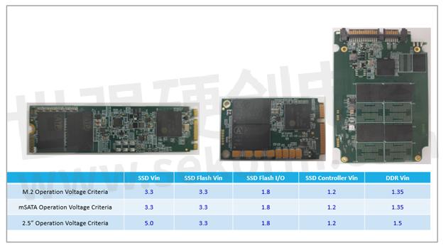
Table 1. Sample In-Circuit Validation Test results for M.2, mSATA, and 2.5” SSDs
●SSD Functional Test Verification. Uses the ATP Gym & Coach System to verify PCB functionality after burn-in using Read-Write test patterns on SSDs.
Test Benchmark: ATP Gym & Coach System
Test Condition: 10 full SSD capacity loops
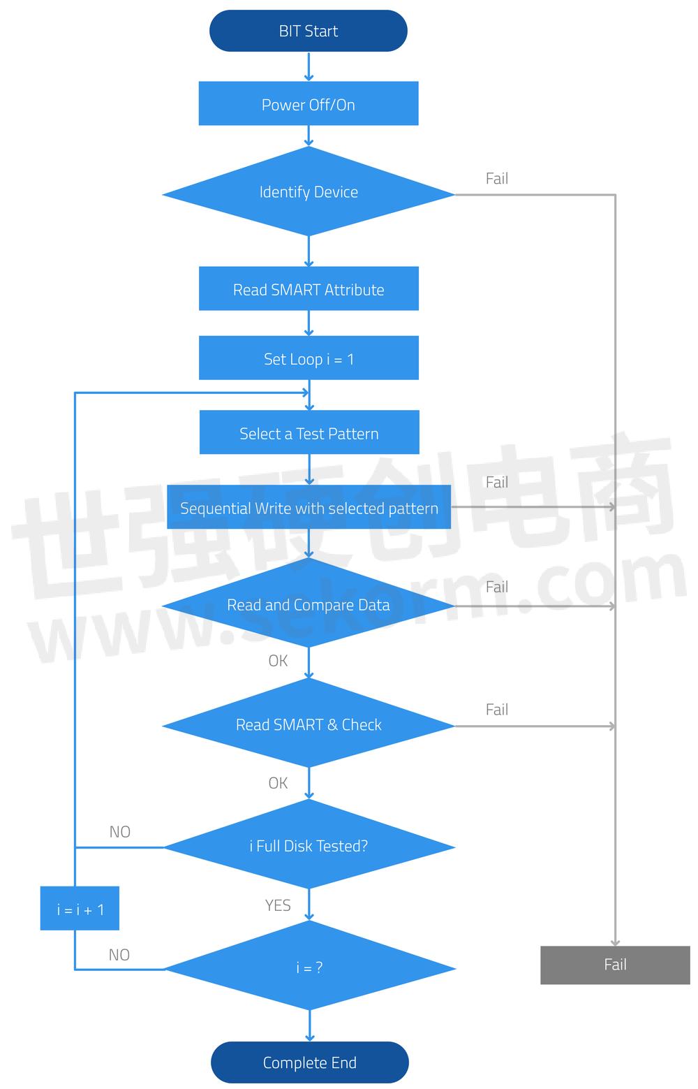
Figure 3. SSD Functional Test Process Flow
●Thermal Cycling Test. This test is used to determine the PCB’s resistance to extreme temperatures. By thermally stressing the PCB solder balls, flaws such as solder joint cracks, warps, lead damage, and other defects can be detected.
ATP performs the thermal cycling test between 0°C to 100 °C for 1000 cycles, with an interim check performed on the 500th cycle. The temperature is ramped up at 14°C per minute, with the PCB dwelling at each extreme temperature level for 10 minutes.
●Shock and Vibration Tests. In many embedded and industrial applications, PCBs are subjected to severe conditions, such as shock and vibration, that can damage the boards themselves or the components on them, compromising the physical, mechanical and electrical integrity of the PCB.
ATP performs these shock and vibration tests to make sure that the PCBs can endure such conditions.
●Non-Operational Random Vibration
●Non-Operational Half-Sine Shock
●Non-Operational Square Wave Shock
●Dye & Pry. This test is used to detect any defects on the solder ball and ball-to-pad interfaces. A dye is infused on the PCB, forcing the dye to penetrate cracks in the solder joints or on the PCB. The PCB is then dried in an oven to prevent the dye from smearing. The board is then mechanically pried to check for the presence of the dye in solder joints/balls or under the solder pads.
Pass/Fail Criteria: Follow IPC-A-610 specifications
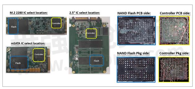
Figure 4. Dye and Pry's results on sample SSDs tested to show that there are no cracks (red dye penetration) on the solder joint and soldering ball.
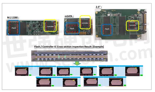
●Cross-Section Check. Also called micro-section analysis, the cross-section test inspects the internal quality of the PCB and provides an interconnection defect analysis. It helps detect internal failures, such as those related to soldering and plating, as well as the thickness of the board layers.
Pass/Fail Criteria: Intermetallic Compound (IMC) layer, soldering status check (Examples: no wetting, cold soldering, dewetting, and others)
Key Takeaways
Soldering defects can affect the functionality of the PCB assembly. This is why ATP takes great care in making sure that all PCB components are effectively bonded through the soldering process. ATP evaluates solderability through rigorous tests, such as visual inspection, thermal cycling, shock and vibration, dye and pry, and cross-section check.
ATP’s PCB assembly validation tests are part of the many reliability and endurance tests developed and performed by ATP to ensure strict compliance to the highest standards of quality. ATP is committed to delivering high-performance and high-endurance NAND flashes storage products to ensure the best value for the total cost of ownership (TCO).
- +1 Like
- Add to Favorites
Recommend
This document is provided by Sekorm Platform for VIP exclusive service. The copyright is owned by Sekorm. Without authorization, any medias, websites or individual are not allowed to reprint. When authorizing the reprint, the link of www.sekorm.com must be indicated.


