XRTC252012S2R2MBCA Integrated Inductor Introduced by Xiangru Electronics Has a DC Resistance as Low as 55mΩ, Realizing Low Loss

Outline
Miniaturization design of electronic products has become the consensus of the current development of electronic industry, which not only meets the consumer's demand for portability and aesthetics, but also drives the development of its internal electronic components to be compact and efficient. In the process of miniaturization of electronic products, engineers are faced with many challenges, such as heat dissipation, power consumption, signal interference, noise and so on. As a result, the miniaturized integrated inductor XRTC252012S2R2MBCA of XIANGRU ELECTRONICS came into being. Its characteristics of small volume, high saturation current, electromagnetic shielding and low loss are suitable for all kinds of miniaturized products with strict requirements on product volume, which can well solve the problems of small product volume, high power density of power supply and electromagnetic compatibility that engineers have a headache.
Typical application circuit
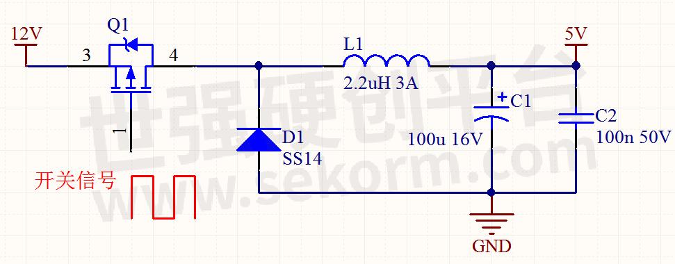
Figure 1 Typical application circuit diagram
This type of inductor is suitable for all kinds of switching power supply circuits, as shown in Figure 1, which is a typical BUCK application circuit. Brief introduction of simple working principle: When Q1 is on, it charges L1 inductor and capacitor C1. When Q1 is off, because the inductor current does not suddenly change, it forms back electromotive force, and C1 is continuously charged through freewheeling diode D1 to maintain the stability of power supply.
Product features
Low DC resistance (typical value is 55mΩ, maximum value is 65mΩ) to realize low loss.
High saturation current (typical 3.8A, maximum 3.3a).
Adopt shielding design to reduce the difficulty of EMI design of products.
The surface adopts vinyl thermal spraying process, which has good surface compactness.
100% lead-free process, meeting RoHS2.0, halogen-free, REACH and other standards.
Application
DC/DC power supply,
PAD, smart phone, portable game device, smart wear,
WI-FI module, notebook, VR, AR,
CD display, HDDS, DVCS, DSCS,
Baseband power supply, amplifier, power supply module, camera power supply and so on.
Appearance and size
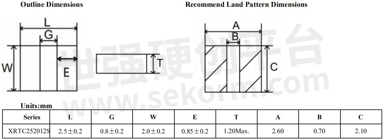
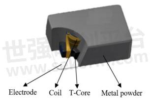
Fig. 3 Structural process
This type of inductor is produced by integrated molding process. The miniaturized integrated molding process has the following advantages:
Miniaturization: The integrated inductor is made of iron core, coil and other components at one time through precise molding process, realizing the extreme miniaturization of components. This design makes the inductor occupy less space, and at the same time, it can meet the pursuit of thinness and portability of modern electronic equipment.
Light weight: Compared with the traditional inductor, the integrated inductor can reduce the weight while maintaining excellent electrical performance, which is helpful to improve the portability and user experience of the whole product.
Specification parameter
The electrical specification parameters of XRTC252012S2R2MBCA are shown in figure 1.

Fig. 4 XRTC25012S2R2MBCA electrical parameters
Under the test frequency of 1MHz, the inductance of this model is stable at 2.2μH tolerance of 20%, which is suitable for DC-DC power supply with high switching frequency. This value is selected according to the actual switching frequency and output current of the power chip.
Low DC impedance, with a typical value of 55mΩ and a maximum value of 65mΩ, greatly reduces the power loss of the inductor itself. According to the formula P=I²*R=2*2*65mΩ=260mW, calculated by 2A effective current. While reducing its own loss, it improves the conversion efficiency of power supply. Now the country is advocating energy saving, and the conversion efficiency index of switching power supply is getting higher and higher. Therefore, the smaller the DC impedance of the inductor, the better.
The maximum rated current of temperature rise is 2.7A, and high rated current can improve the power density of DC-DC power supply module. The design of this value needs to consider the derating design, and the derating factor is preferably 0.7.
The maximum saturation current is 3.3A, which reflects the maximum energy storage of the inductor. Small volume and high saturation current can make the power design range of products wider, cover multiple product power sections, and realize the standardization of materials to the greatest extent.
Naming rules for product models
The naming rules of this model product series are shown in Figure 5. XRTC252012S2R2MBCA model indicates: miniaturized integrated inductor, length and width 2.5*2mm, height 1.2mm, structural dimension tolerance ±0.2mm, inductance 2.2μH, inductance tolerance 20%, universal conventional inductor. If the technical parameters of this inductor are not applicable, you can contact to apply for samples according to the series naming rules.
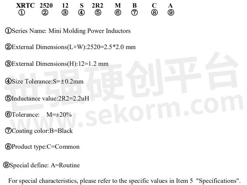
Figure 5 product model naming rules
- +1 Like
- Add to Favorites
Recommend
This document is provided by Sekorm Platform for VIP exclusive service. The copyright is owned by Sekorm. Without authorization, any medias, websites or individual are not allowed to reprint. When authorizing the reprint, the link of www.sekorm.com must be indicated.


