Ultra-Wide-Body Digital Isolators Make High-Voltage Applications More Efficient and Reliable
In recent years, the number of photovoltaic systems, chargers, new energy vehicles, energy storage facilities, and other emerging technologies is increasing, and the installed base of industrial control devices, power supply, electricity, and other conventional applications is still climbing. In this setting, high-voltage digital control applications pose growing isolation requirements, and the market sees strong demand for high-efficiency and high-reliability digital isolators accordingly.
In high-voltage systems, a reliable isolation gate must be built using isolation means, which electrically isolates sensitive electronic components from fast transient high-voltage components to ensure power safety, better system performance, and higher reliability. To this end, many factors need to be taken into account, including isolation rating, creepage distance and electric clearance, common-mode transient immunity (CMTI), and electromagnetic interference (EMI).
Wide bandgap (WBG) devices like SiC and driver products pose higher requirements for isolators while continuously improving the power density. Digital isolator now has become one of the semiconductor devices that help unlock the huge potential of high-voltage applications. It is widely used in photovoltaic systems, new energy vehicles, industrial automation systems, isolated SPI, RS232, RS485, general-purpose multi-channel isolation units, and motor control.
Challenges facing high-voltage isolation
The growing requirements for higher reliability, longer service life and higher signal integrity in industry and automotive fields present challenges for high-voltage applications.
High voltage power conversion must enhance efficiency while minimizing the system power loss. High voltage isolation design requires a robust isolation barrier to ensure system security. Under harsh operating conditions, it is necessary to address the difficulty in accurately measuring temperature, current, and voltage by high voltage sensors.
In addition, the use of WBG power devices also makes low-delay real-time control of high-voltage systems essential. As the electrification process advances and high-voltage power systems become more complex, designers need to consider how to improve product performance and service life while ensuring the right isolation level and system security.
A digital isolator is a device that enables signal transmission in electrical isolation conditions. Featuring high operating voltage, low radiation, low power consumption, and high efficiency, it is extensively used in industrial control, electric energy, communication networks, instrumentation, consumer electronics, and other electronic systems and devices.
At present, three mainstream isolation solutions are available in the market: optocouplers, capacitive isolators, and magnetic isolators.
Optocoupler came as the earliest isolation technology. It uses optical characteristics to realize one-way transmission of signals. However, due to optical attenuation over time, optocouplers may experience the aging effect.
Capacitive isolator uses the capacitance effect to eliminate cross interference between signals and features low propagation delay. It can transmit data at a rate of more than 150Mbps and consumes less bias current. However, a capacitive isolator requires separate bias supply voltages on both sides of the isolation boundary. The biggest advantage of the capacitive isolator is that it is low-cost and can adopt a multichannel design.
Magnetic isolator isolates signals by shielding the magnetic field. This makes it advantageous in applications requiring high-frequency DC-DC power conversion, but it is relatively expensive.
Ultra-wide-body package emerging at the right time
In photovoltaic applications, monocrystalline silicon and polycrystalline silicon materials are required. To improve the power density of photovoltaic modules, the bus voltage has been increased to 1500 V. This requires an isolator that provides a longer creepage distance to meet the voltage withstand and creepage distance requirements specified in China’s national standard GB4943.1-2022. As a response, some wide-body (SOP) and even ultra-wide-body (DWW) packages emerged. Different manufacturers designate different names for ultra-wide-body packages.
An ultra-wide-body digital isolator is a highly reliable isolation product that features high electromagnetic immunity, low electromagnetic radiation, and low power consumption, and can withstand higher isolation surge voltage. The creepage distance of the ultra-wide-body package is up to 15 mm, which can meet the safety requirements of customers’ high-voltage systems. In photovoltaic systems, for example, the creepage distance of the isolator under 1500V enhanced insulation condition shall be more than 14 mm, as required in IEC 62109.
NSI82xx digital isolators from NOVOSENSE are products in the ultra-wide-body packages. They provide a long creepage distance of 15mm and an outstanding EMC property. This makes this digital isolator series a perfect choice for photovoltaic facilities and other high-voltage systems having a high creepage distance requirement. Moreover, the NSI82xx series is compatible with high-precision, high-speed, and two-way digital isolators from other manufacturers, such as ISO78xx, ISO774x-Q1, ACNT-H6xL, etc.
Depending on applications, the NSI82xx series is divided into two sub-series – NSI82xx-DSWWR and NSI82xx-Q1SWWR high-reliability, multichannel Ultra-wide-body digital isolators. NSI82xx-DSWWR sub-series is designed for industrial applications, including NSI822xWx-DSWWR (2-channel), NSI823xWx-DSWWR (3-channel), and NSI824xWx-DSWWR (quad-channel). NSI82xx-Q1SWWR sub-series is suitable for automotive applications, including NSI822xWx-Q1SWWR (2-channel), NSI823xWx-Q1SWWR (3-channel), and NSI824xWx-Q1SWWR (quad-channel).
According to the available information, NSI82xx-DSWWR ultra-wide-body digital isolators started mass production in January 2022, and a total of more than one million devices have been sold currently. More specifically, customers from power supply, NEVs, electric power, industrial control, photovoltaic, energy storage, and charging piles are using ultra-wide-body digital isolators from NOVOSENSE.
Answering high efficiency, high reliability, and multi-function requirements
For example, the quad-channel NSI824x digital isolator has UL1577 safety approval and can withstand several levels of insulation voltage (3 kVrms, 3.75 kVrms, 5 kVrms, and 8 kVrms). It’s noted that the ultra-wide-body package provides insulation voltage withstand capability of up to 8 kVrms, data rate of up to 150 Mbps, and CMTI of up to 200kV/μs (min.).
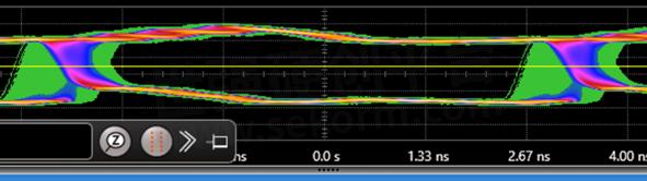
Eye diagram showing high-speed performance of NSI824x
The NSI824x device provides digital channel direction configuration and the default output level configuration when the input power is lost. Thanks to a wide supply voltage range, NSI824x can be directly connected with most digital interfaces and allows easy level shift. Moreover, high system level EMC performance enhances its reliability and stability in service.
The NSI824x series adopts the capacitive isolator technology, where the digital signal is modulated by the RF carrier generated by the internal oscillator on the transmitter side, then transmitted via the capacitive isolator and demodulated on the receiver side. It’s especially noted that the proprietary Adaptive OOK® modulation technology from NOVOSENSE is used, which delivers many benefits including high noise resistance and low EMI.
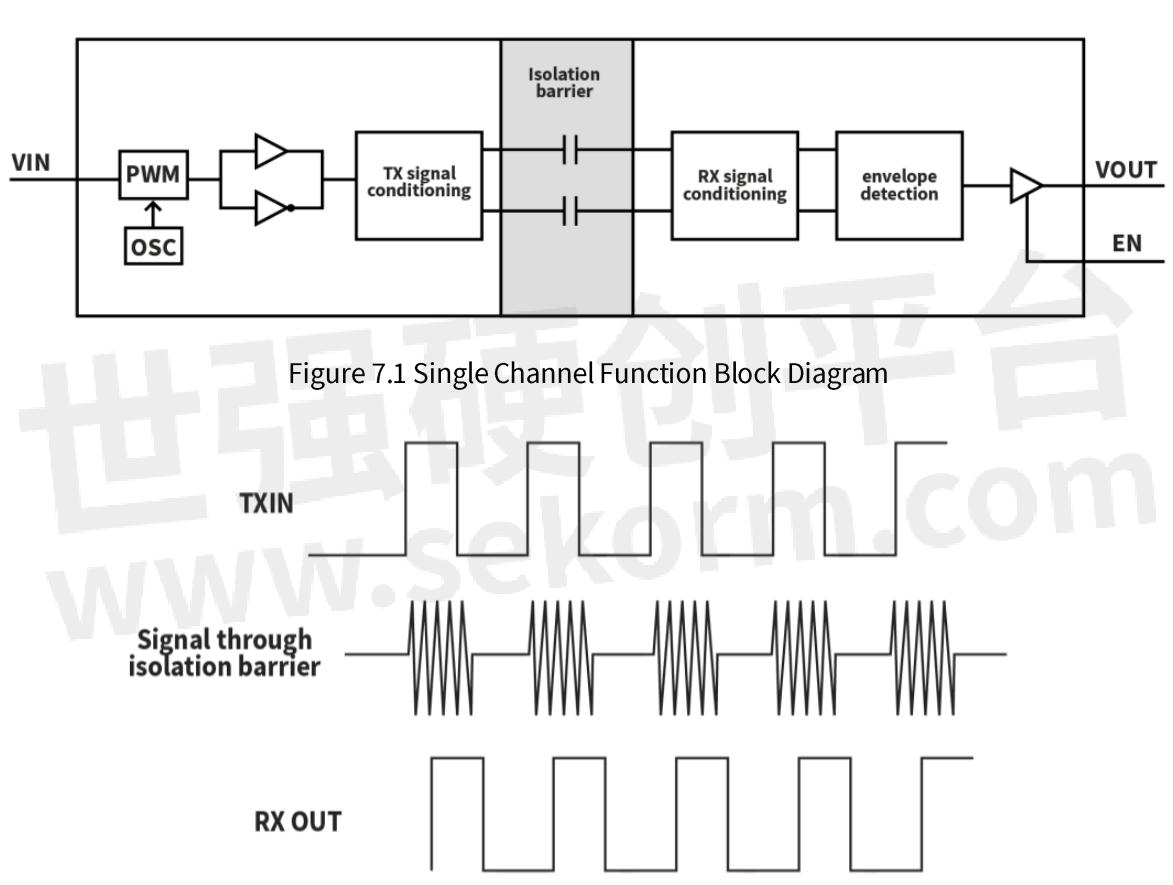
Functional block diagram of the single-channel device and OOK modulation
Key features
NSI824x digital isolators have rich functional features as described below:
Insulation voltage: Up to 8kVrms (Ultra-wide-body package)
Data rate: DC to 150Mbps
Power supply voltage: 2.5V to 5.5V
High CMTI: 200kV/μs (min.)
Chip level ESD: ±8kV (human body model)
Robust electromagnetic compatibility (EMC)
System-level ESD, EFT, and surge immunity
Low electromagnetic radiation
Default output high level or low level option
Low power consumption: 1.5mA/ch (1Mbps)
Low propagation delay: <15ns
Operating temperature: -55℃-125℃
RoHS-compliant packages:
SOP16 (150mil), SSOP16, SOP16 (300mil) and SOP16 (600 mil)
Part number, package, and body size
NSI824x digital isolators have the following safety regulatory approvals:
UL1577 recognition: Insulation voltage up to 8kVrms for 1 minute
CQC certification per GB4943.1-2011
CSA component notice 5A
DIN VDE V 0884-11:2017-01 enhanced isolator certification
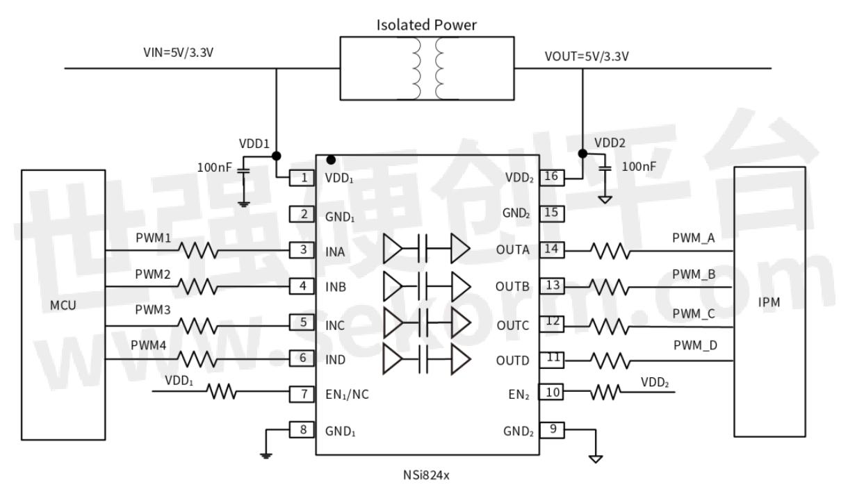
IPM's typical PWM isolated circuit
Tips for PCB layout
In the PCB layout, it should be noted that a 0.1μF bypass capacitor is required between VDD1 and GND1, and between VDD2 and GND2 of the NSI824x device and that the capacitor should be placed as close to the package as possible. In the front of the recommended PCB layout, it should be ensured that there are no planes, traces, bonding pads, and via holes in the space under the chip.
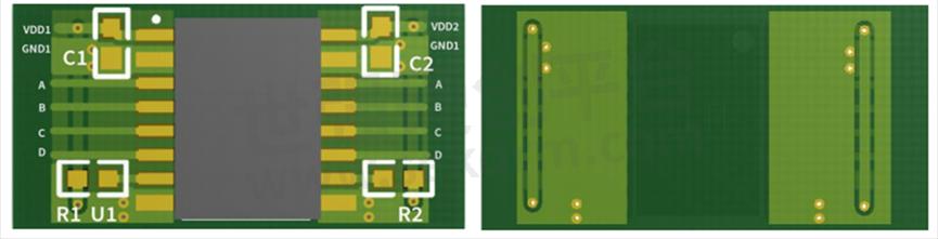
Front and back of recommended PCB layout
In case of excessively high system noise, users can also place a resistor (50-300Ω) connected in series with the input and output for enhanced robustness of their design. A series resistor can also improve system reliability, for example, latch-up immunity. The typical output impedance of the isolator drive channel is about 50Ω (±40%). When the drive transmission line affects the load, the output pin should be appropriately terminated with a PCB trace having controlled impedance.
- +1 Like
- Add to Favorites
Recommend
This document is provided by Sekorm Platform for VIP exclusive service. The copyright is owned by Sekorm. Without authorization, any medias, websites or individual are not allowed to reprint. When authorizing the reprint, the link of www.sekorm.com must be indicated.
Integrated Circuits


Discrete Components


Connectors & Structural Components


Assembly UnitModules & Accessories


Power Supplies & Power Modules


Electronic Materials


Instrumentation & Test Kit


Electrical Tools & Materials


Mechatronics


Processing & Customization


