Dual P-Channel MOSFET CJ3139KDW, Using Advanced Power Trench Process to Optimize the RDS(ON)

This JSCJ Dual P-Channel MOSFET CJ3139KDW has been designed using advanced Power Trench process to optimize the RDS(ON). Including two P-ch CJ3139K MOSFET (independently) in a package.
FEATURE
High-Side Switching
Low On-Resistance
Low Threshold
Fast Switching Speed
APPLICATION
Drivers: Relays, Solenoids, Lamps, Hammers, Displays, Memories
Battery Operated Systems
Power Supply Converter Circuits
Load/Power Switching Cell Phones, Pagers
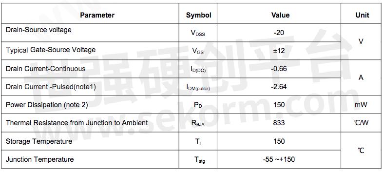
Maximum ratings (Ta=25℃ unless otherwise noted)
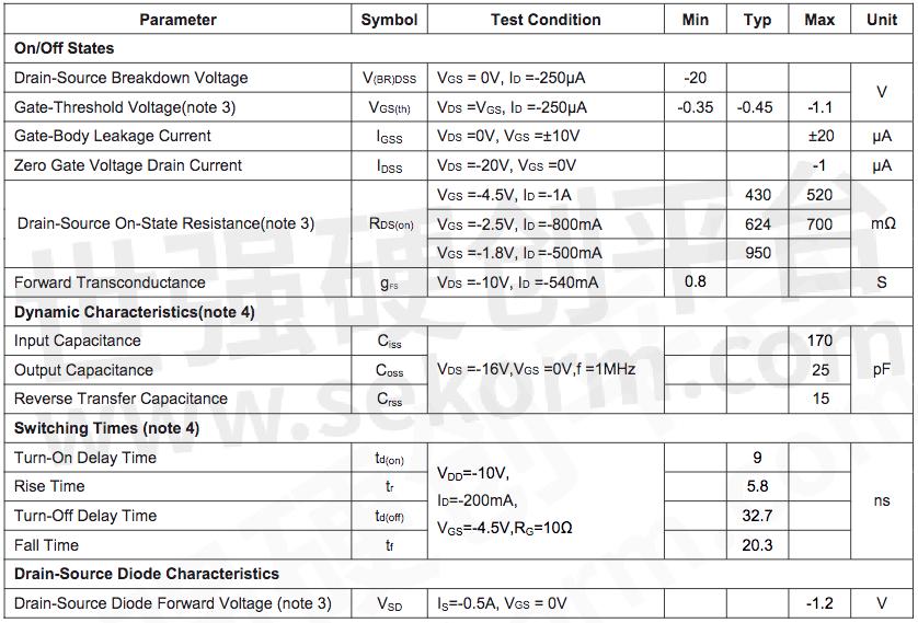
ELECTRICAL CHARACTERISTICS (Ta=25℃ unless otherwise specified)
Notes:
1. Repetitive Rating: Pulse width limited by maximum junction temperature.
2. This test is performed with no heat sink at Ta=25℃.
3. Pulse Test : Pulse Width≤300μs, Duty Cycle≤0.5%.
4. These parameters have no way to verify.
MARKING
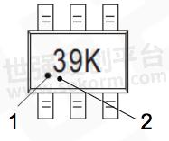
39K=Device code
Solid dot1=Pin1 indicator
Solid dot2= Green molding compound device.
- +1 Like
- Add to Favorites
Recommend
- SOT-23 Plastic-Encapsulate Diodes ESD36VAP, Features with a Reverse Stand−off Voltage of 36V and a Fast Response Time
- Bi-direction ESD Protection Diode ESDBVD5V0C2 for Applications such as HDMI, Display Port TM, and MDDI Interfaces
- Low Dropout Linear Regulator CJT1117B-XXX with A Dropout of 1.15V(typ.) at 1A Output Current
- Bi-direction ESD Protection Diode ESDBM12VD3 with Excellent Clamping Capability, Low Leakage, Low Capacitance and Fast Response Time
- Bi-direction ESD Protection Diode ESDBL18VD3 with a Low Reverse Stand−off Voltage of 18V and a Low Reverse Clamping Voltage
- Bi-direction ESD Protection Diode ESDBNC3V3B1 with a Low Reverse Stand−off Voltage of 3.3V and Small Size
- Bi-direction ESD Protection Diode ESDBKV15VD3, Features with a Low Capacitance of 2pf and a High Level of ESD Protection
- Explore How to Choose a Dual Polarized Vivaldi Antenna and Introduce the Kinghelm Vivaldi Antenna, 6G Dual Polarized Vivaldi Antenna KH-6G-0H-08
This document is provided by Sekorm Platform for VIP exclusive service. The copyright is owned by Sekorm. Without authorization, any medias, websites or individual are not allowed to reprint. When authorizing the reprint, the link of www.sekorm.com must be indicated.
Integrated Circuits


Discrete Components


Connectors & Structural Components


Assembly UnitModules & Accessories


Power Supplies & Power Modules


Electronic Materials


Instrumentation & Test Kit


Electrical Tools & Materials


Mechatronics


Processing & Customization


