Addressing Device Modeling Challenges for Advanced Technologies
In most domains, a million is a large number.
But in the realm of device modeling, a hundred billion is normal, with expectations of trillion-transistor chips by 2030 becoming commonplace.
The intricacies of modeling advanced semiconductor devices present formidable complexity and time demands. Engineers must extract hundreds of parameters to accurately capture the RF behavior of the device across various sizes and temperatures. With the process technology advancing towards 2nm and below, smaller device sizes introduce additional unforeseen effects at the nanoscale, uncharted in older technologies. In this interview, we sit down with Sherry Lyu, Device Modeling Solution Engineer at Keysight, to gain her insights into the device modeling challenges on the path to 2nm and beyond.
What does device modeling entail?
Device modeling is the art and science of creating mathematical and physical models to describe the intricate behavior of individual semiconductor devices, such as transistors, diodes, and capacitors under various conditions.
These models provide electronic designers with critical insights into how these components will perform in real-world applications.
Modeling remains a key enabler of the design flow. Let's take the simplest example of a resistor model. Suppose we have a set of measured data for current and voltage (V, I), which follows a linear, I=V/R. By adjusting the parameter R, the best-fit results with the data points can be obtained when R=R0.
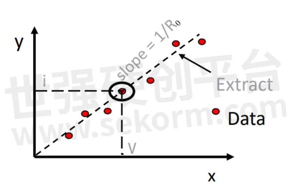
Figure 1. A simplified version of the resistor model
This example illustrates two steps of modeling: the first step is to find the right physics equation, and the second step is parameter extraction. The concept is similar for modeling semiconductor devices like MOSFETs, BJTs, and Diodes, except that the equations describing the characteristics of these devices are more complex.
Why an accurate device model is important?
With an accurate model, design engineers can optimize their designs to meet specific requirements, whether it's maximizing speed, minimizing power consumption, or ensuring reliability.
By simulating device behavior under different conditions, engineers can effectively reduce the need for expensive physical prototypes, thereby saving tremendous time and resources. For instance, in contexts where power electronics are assuming increasingly pivotal roles, such as in electric vehicle applications, there is a growing demand for highly accurate models tailored to power devices like IGBTs, power MOSFETs, and diodes.
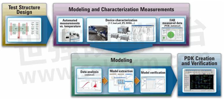
Figure 2. Device modeling flow
Most importantly, accurate models empower researchers to explore new materials and structures, fostering innovation in semiconductor technology and pushing the boundaries of what's possible. Consider, for example, the emerging technologies like memristors necessitate the development of new compact models to comprehensively understand their distinctive characteristics and enable seamless integration into complex circuit designs.
Samsung recently announced using Keysight's RF Device Model Generator to accelerate modeling flow. Can you tell us more about it?
This milestone builds on our numerous successful collaborations with Samsung and innovates the next-generation transistor technology. Leveraging our advanced IC-CAP (Integrated Circuit Characterization and Analysis Program), Samsung's RF modeling engineers can efficiently organize large volumes of data, resulting in significant time savings during the process of extracting models. Our software manages complex netlists and the variety of measured data (including S-parameters and low- and high-frequency noise), and all the details of simulating and displaying multi-device simulations, realizing efficiency gains of at least 30 percent.
Furthermore, our latest innovation introduces an integrated model recentering tool, taking efficiency to the next level. Whether it involves essential metrics such as threshold voltage, cutoff frequency, or other FOMs, modeling engineers now can modify existing models to align with new specifications, with potential efficiency gains of up to 70 percent compared to traditional step-by-step model extraction methodologies.
Are you seeing an increasing need for advanced modeling solutions?
Absolutely. With the CHIPS Act infusing $280 billion into domestic semiconductor research and manufacturing in the United States, the demand for SPICE models for cutting-edge technologies is escalating. This influx of demand places heightened pressure on modeling teams at foundries of all sizes. Ensuring efficiency while upholding model quality has become a top priority.
Are there any disruptive technologies on the horizon that you foresee as significant?
From my point of view, Artificial Intelligence and Machine Learning (AI/ML) hold tremendous promise and have the potential to bring about a significant advancement in modeling precision and efficiency. Today’s circuit simulation relies on an industry-standard compact model. However, developing a new compact model for next-generation devices is very complicated, which requires the involvement of numerous experts and typically spans several years. To address the lack of compact models, researchers are developing new modeling methodologies that leverage AI/ML techniques to predict the performance of emerging devices.
What is Keysight doing to leverage AI/ML for device modeling?
We are working very closely with the device modeling communities and leading industry and academic experts to advance EDA tool flows for AI/ML.
Our Artificial Neural Network (ANN) solution empowers modeling engineers to enhance model accuracy through an IC-CAP Python script, streamlining ANN training, evaluation, and Verilog-A model export. The input for ANN training can span any number of dimensions (e.g., Vg, Vd, T). Instead of relying solely on traditional physics or equation-based compact models, ANN models are employed for extraction. This process is fully automated, delivering results faster and more efficiently. The output can either be in the form of an equation or a Verilog-A model, with better and faster convergence compared to some detailed compact models. The ANN solution proves instrumental in scenarios where no compact model exists for new technologies or where existing models fall short and a rapid device model generation is necessary.
Conclusion
As our industry moves to 2nm and beyond, it will require a new level of innovation and collaboration to achieve success.
Keysight’s IC-CAP is ideally positioned to lead this effort with our partners across foundries, research institutions, and industry leaders to overcome new modeling challenges and drive the new wave of the semiconductor revolution.

Join Sherry and other device modeling experts to learn advanced methods for on-wafer measurements and modeling on Nov.8 at FormFactor San Jose Demo Center.
- +1 Like
- Add to Favorites
Recommend
- Keysight Technologies Acquires Quantum Benchmar, Augmenting Keysight‘s Quantum Portfolio
- Keysight First to Gain OmniAir Qualified Test Equipment Status, Accelerating C-V2X Device Certification
- Keysight First to Gain GCF Approval of Cases for Validating 5G New Radio mmWave Devices in Standalone Mode
- Keysight Massively Parallel Board Test System Selected by LACROIX in Automotive Printed Circuit Board Manufacturing
- Keysight, TIM and JMA Wireless Join Forces to Showcase O-RAN Technology at Mobile World Congress 2021
- Keysight, Xilinx and Cisco Showcase Solutions that Support Smooth Migration from 4G LTE Networks to 5G Open RAN
- Keysight Unveils the First Media Access Control Security Test Solution for High Speed Ethernet
- Keysight, MediaTek Join Forces to Establish 5G Connectivity Based on 3GPP Release 16 Specifications
This document is provided by Sekorm Platform for VIP exclusive service. The copyright is owned by Sekorm. Without authorization, any medias, websites or individual are not allowed to reprint. When authorizing the reprint, the link of www.sekorm.com must be indicated.
Integrated Circuits


Discrete Components


Connectors & Structural Components


Assembly UnitModules & Accessories


Power Supplies & Power Modules


Electronic Materials


Instrumentation & Test Kit


Electrical Tools & Materials


Mechatronics


Processing & Customization


