Design Considerations for Building Robust Circuit Protection in Electrified and Increasingly Automated Vehicles

Designing circuits for electrified vehicles is extremely challenging. To ensure robust and safe designs that can withstand overloads, transients, and electrostatic discharge (ESD), designers need to ensure their circuits have the necessary components that will prevent damage. This article presents recommendations for both circuit protection and efficient control using the on-board charger as an example circuit.
Hybrid vehicles, as seen in the Fig. 1 schematic, represent the worst-case scenario for designers who must develop circuitry that can withstand transients from both the internal combustion engine and the high-power electric motors. In this environment, the on-board charger must contend with the AC power line and its potential for generating overloads and transients.

Fig.1. In hybrid-electric vehicle electrical architectures, the on-board charger must contend with the AC power line and its potential for generating overloads and transients. (Littelfuse)
Designers should protect the on-board charger just as they would protect any line-powered product. They also will want to protect communication circuits to avoid corruption of data while minimizing internal power consumption, so that battery charge time is as short as possible.
The on-board charger converts the AC line voltage into the DC voltage required for charging the main battery pack which, when fully charged, can contain voltage in the range of 300 to 500 V. Consumers want faster EV charging, thus the demand for higher-power charging circuits which can include 3-phase power.
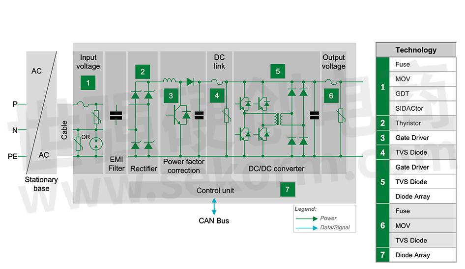
Fig. 2 shows a block diagram of an on-board charger. In this example, a single-phase circuit is represented. Each circuit block requires protection components, and two blocks require control components to optimize the charger for efficiency.

Fig.2.On-board charger block diagram and recommended protection and control componets
MOVing to transient protection
The input voltage section is susceptible to transients such as a lightning strike and surges on the AC line. The first line protection is a fuse to provide overload protection. Designers should consider fuses with a high interrupting current rating and a high voltage rating to ensure the fuse will open under the worst-case current overload. To protect against a surge transient or a lightning strike, designers should place a metal oxide varistor (MOV) as close to the input connections of the charger as possible. The MOV will absorb the transient energy and can prevent it from damaging the downstage circuit blocks.
If the on-board charger uses 3-phase power, the designer should consider adding MOVs for phase-phase transient protection as well as phase-neutral transient protection. For even greater protection of downstream circuits, designers can place a bipolar thyristor in series with the MOV. A thyristor has a very low clamping voltage of around 5 V. Use of a thyristor allows a designer to select an MOV with a lower standoff voltage. The net effect is the reduction of the peak transient voltage to which the downstage circuitry is momentarily subjected.
A fourth protection element for superior circuit protection is a gas discharge tube. The gas discharge tube provides high resistance, electrical isolation between the hot and neutral lines and the vehicle’s chassis ground. Gas discharge tubes provide an additional level of protection against fast-rising transients from lightning disturbances.
IGBTs to the rescue
For fast, high power charging, designers should select rectifier block thyristors with sufficient current handling capacity to supply the necessary power. Thyristors also can absorb safely surge current transients that may have passed through the input voltage and EMI filter stages.
The power factor correction (PFC) circuit improves the efficiency of the charge by reducing the total power drawn from the AC power line. Designers can use a gate driver and an insulated gate bipolar transistor (IGBT) to control the amount of inductance in the circuit. Designers should ensure that they select a gate driver with a sufficient operating voltage range for control of the IGBT. Designers also should consider selecting a gate driver with high immunity to latch-up and with fast rise-and-fall times to quickly switch the IGBT.
Fast rise-and-fall times combined with a low supply current minimize power consumption of this circuit block. The gate driver should be protected from ESD; designers should either select a gate driver with built-in ESD protection or add an external ESD diode. Versions of ESD diodes can be either bi-directional or uni-directional and can withstand ESD transients as high as 30 kV.
Know the key diodes
The DC link consists of the capacitor bank that stabilizes the ripple generated by the high-power DC/DC converter. Designers concerned about large voltage transients reaching the DC link can employ a high-voltage TVS diode to protect the capacitor bank.
The DC/DC section steps up the output charge voltage and generates the charge current for the battery. This circuit block requires a robust gate driver similar to the PFC circuit block. If a gate driver selection does not include internal ESD protection, designers can select an ESD diode to protect the gate driver. Addition of an external ESD diode does not degrade the performance of the gate driver.
Designers should also ensure that their power IGBTs are protected from voltage transients. In addition to protection from external transients, the IGBT creates turn-off switching transients due to L·di/dt effects from internal parasitic inductance (L being the inductance and di/dt the rate of current change). To eliminate the potential damage to an IGBT from this transient, designers should place a TVS diode between the collector and gate of each IGBT.
The TVS diode reduces the di/dt of the current transient by raising the gate voltage. When the collector-emitter voltage exceeds the breakdown voltage of the TVS diode, current flows through the TVS diode into the gate to raise its potential. The TVS diode continues to conduct until the transient is eliminated.
Use of a TVS diode as a collector-gate feedback element is known as active clamping and keeps the IGBT in a stable state. More information on active clamping is available in the referenced application note.1 Some IGBTs have built-in active clamping TVS diodes. Designers either should select that type of IGBT or add TVS diodes to their circuit.
Protecting CAN bus signals
The output voltage stage requires protection from current overloads and in-vehicle voltage transients when motors turn on and off or when current is instantaneously interrupted by a break in a cable. Designers should consider employing a fuse to protect from an overcurrent resulting from a short in the battery pack or in the cables that carry the battery voltage. Use of an MOV or a TVS diode protects against the potentially damaging voltage transients.
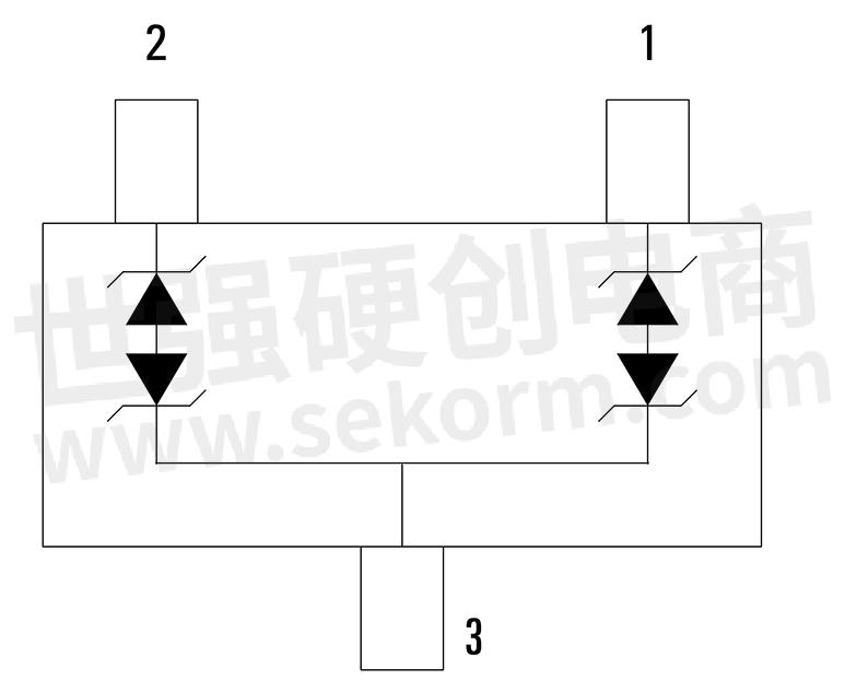
The control unit for the charger communicates with the data network via the CAN bus. To avoid damage to the communication circuit block and avoid corruption of data, designers should provide ESD and transient protection. They can implement the protection with a single, space-saving component. Fig. 3 shows a dual-line TVS diode array designed for protection of CAN bus signal lines. Diode arrays designed for protecting communication lines contain minimal capacitance and do not degrade the transmitter/receiver I/O states.

Fig.3.TVS diode array for protection of CAN bus lines
Designers who follow the recommendations for protection and control will have robust, reliable and safe circuits for their companies’ EV customers. Whenever possible, designers should use AEC-Q qualified components that have been certified for use in the automotive environment. For example, AEC-Q101 covers discrete semiconductors, and AEC-Q200 covers passive components such as varistors. Furthermore, designers should consider taking advantage of the manufacturers’ experts for assistance in selection of appropriate protection components.
- +1 Like
- Add to Favorites
Recommend
This document is provided by Sekorm Platform for VIP exclusive service. The copyright is owned by Sekorm. Without authorization, any medias, websites or individual are not allowed to reprint. When authorizing the reprint, the link of www.sekorm.com must be indicated.


